


MII_TXCLK
MII_TXD[3−0]
MII_TXEN
MII_COL
MII_CRS
MII_RXCLK
MII_RXD[3−0]
MII_RXDV
MII_RXER
MDIO_CLK
MDIO_D
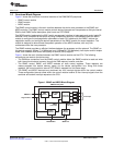
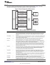
Physical
layer
device
(PHY)
System
core
Transformer
2.5 MHz
or
25 MHz
RJ−45
EMACMDIO
www.ti.com
Architecture
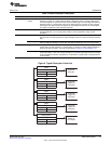
The individual EMAC and MDIO signals for the MII interface are summarized in Table 1. For more
information, refer to either the IEEE 802.3 standard or ISO/IEC 8802-3:2000(E).
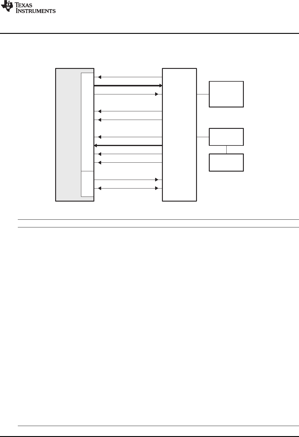
Figure 2. Ethernet Configuration—MII Connections
Table 1. EMAC and MDIO Signals for MII Interface
Signal Type Description
MII_TXCLK I Transmit clock (MII_TXCLK). The transmit clock is a continuous clock that provides the timing
reference for transmit operations. The MII_TXD and MII_TXEN signals are tied to this clock. The
clock is generated by the PHY and is 2.5 MHz at 10 Mbps operation and 25 MHz at 100 Mbps
operation.
MII_TXD[3-0] O Transmit data (MII_TXD). The transmit data pins are a collection of 4 data signals comprising 4 bits
of data. MTDX0 is the least-significant bit (LSB). The signals are synchronized by MII_TXCLK and
valid only when MII_TXEN is asserted.
MII_TXEN O Transmit enable (MII_TXEN). The transmit enable signal indicates that the MII_TXD pins are
generating nibble data for use by the PHY. It is driven synchronously to MII_TXCLK.
MII_COL I Collision detected (MII_COL). In half-duplex operation, the MII_COL pin is asserted by the PHY
when it detects a collision on the network. It remains asserted while the collision condition persists.
This signal is not necessarily synchronous to MII_TXCLK nor MII_RXCLK.
In full-duplex operation, the MII_COL pin is used for hardware transmit flow control. Asserting the
MII_COL pin will stop packet transmissions; packets in the process of being transmitted when
MII_COL is asserted will complete transmission. The MII_COL pin should be held low if hardware
transmit flow control is not used.
MII_CRS I Carrier sense (MII_CRS). In half-duplex operation, the MII_CRS pin is asserted by the PHY when
the network is not idle in either transmit or receive. The pin is deasserted when both transmit and
receive are idle. This signal is not necessarily synchronous to MII_TXCLK nor MII_RXCLK.
In full-duplex operation, the MII_CRS pin should be held low.
MII_RXCLK I Receive clock (MII_RXCLK). The receive clock is a continuous clock that provides the timing
reference for receive operations. The MII_RXD, MII_RXDV, and MII_RXER signals are tied to this
clock. The clock is generated by the PHY and is 2.5 MHz at 10 Mbps operation and 25 MHz at
100 Mbps operation.
MII_RXD[3-0] I Receive data (MII_RXD). The receive data pins are a collection of 4 data signals comprising 4 bits of
data. MRDX0 is the least-significant bit (LSB). The signals are synchronized by MII_RXCLK and
valid only when MII_RXDV is asserted.
MII_RXDV I Receive data valid (MII_RXDV). The receive data valid signal indicates that the MII_RXD pins are
generating nibble data for use by the EMAC. It is driven synchronously to MII_RXCLK.
MII_RXER I Receive error (MII_RXER). The receive error signal is asserted for one or more MII_RXCLK periods
to indicate that an error was detected in the received frame. This is meaningful only during data
reception when MII_RXDV is active.
15
SPRUFL5B–April 2011 EMAC/MDIO Module
Submit Documentation Feedback
© 2011, Texas Instruments Incorporated