


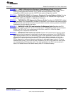
RMII_TXD[1-0]
RMII_TXEN
RMII_MHZ_50_CLK
RMII_RXD[1-0]
RMII_CRS_DV
RMII_RXER
MDIO_CLK
MDIO_D
MDIO
EMAC
Physical
Layer
Device
(PHY)
Transformer
50MHz
RJ-45
Architecture
www.ti.com
Table 1. EMAC and MDIO Signals for MII Interface (continued)
Signal Type Description
MDIO_CLK O Management data clock (MDIO_CLK). The MDIO data clock is sourced by the MDIO module on the
system. It is used to synchronize MDIO data access operations done on the MDIO pin. The
frequency of this clock is controlled by the CLKDIV bits in the MDIO control register (CONTROL).
MDIO_D I/O Management data input output (MDIO_D). The MDIO data pin drives PHY management data into
and out of the PHY by way of an access frame consisting of start of frame, read/write indication,
PHY address, register address, and data bit cycles. The MDIO_D pin acts as an output for all but the
data bit cycles at which time it is an input for read operations.
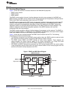
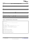
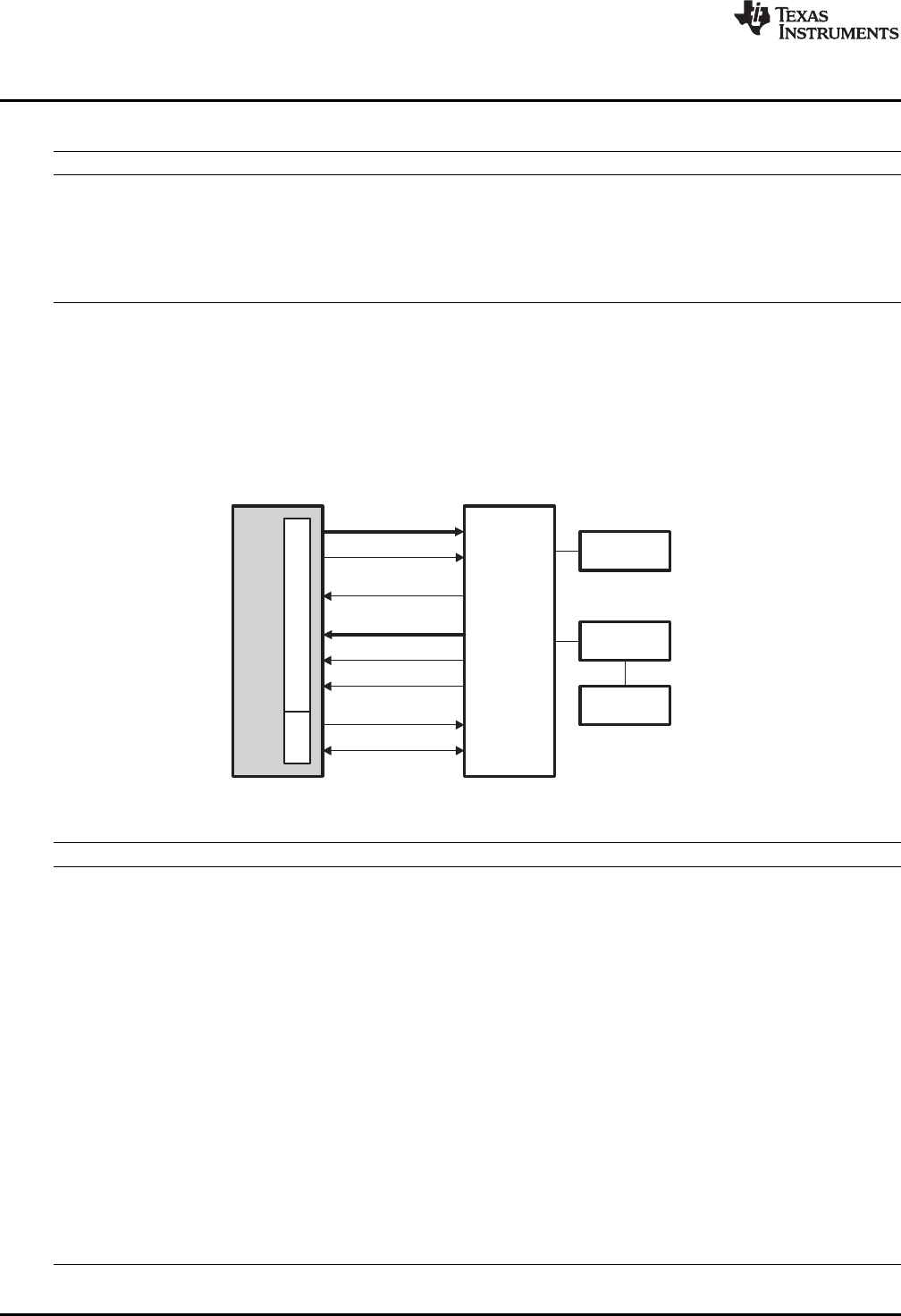
2.3.2 Reduced Media Independent Interface (RMII) Connections
Figure 3 shows a device with integrated EMAC and MDIO interfaced via a RMII connection in a typical
system.
The individual EMAC and MDIO signals for the RMII interface are summarized in Table 2. For more
information, refer to either the IEEE 802.3 standard or ISO/IEC 8802-3:2000(E).
Figure 3. Ethernet Configuration—RMII Connections
Table 2. EMAC and MDIO Signals for RMII Interface
Signal Type Description
RMII_TXD[1-0] O Transmit data (RMII_TXD). The transmit data pins are a collection of 2 bits of data. RMTDX0 is
the least-significant bit (LSB). The signals are synchronized by RMII_MHZ_50_CLK and valid only
when RMII_TXEN is asserted.
RMII_TXEN O Transmit enable (RMII_TXEN). The transmit enable signal indicates that the RMII_TXD pins are
generating data for use by the PHY. RMII_TXEN is synchronous to RMII_MHZ_50_CLK.
RMII_MHZ_50_CLK I RMII reference clock (RMII_MHZ_50_CLK). The reference clock is used to synchronize all RMII
signals. RMII_MHZ_50_CLK must be continuous and fixed at 50 MHz.
RMII_RXD[1-0] I Receive data (RMII_RXD). The receive data pins are a collection of 2 bits of data. RMRDX0 is the
least-significant bit (LSB). The signals are synchronized by RMII_MHZ_50_CLK and valid only
when RMII_CRS_DV is asserted and RMII_RXER is deasserted.
RMII_CRS_DV I Carrier sense/receive data valid (RMII_CRS_DV). Multiplexed signal between carrier sense and
receive data valid.
RMII_RXER I Receive error (RMII_RXER). The receive error signal is asserted to indicate that an error was
detected in the received frame.
MDIO_CLK O Management data clock (MDIO_CLK). The MDIO data clock is sourced by the MDIO module on
the system. It is used to synchronize MDIO data access operations done on the MDIO pin. The
frequency of this clock is controlled by the CLKDIV bits in the MDIO control register (CONTROL).
MDIO_D I/O Management data input output (MDIO_D). The MDIO data pin drives PHY management data into
and out of the PHY by way of an access frame consisting of start of frame, read/write indication,
PHY address, register address, and data bit cycles. The MDIO_D pin acts as an output for all but
the data bit cycles at which time it is an input for read operations.
16
EMAC/MDIO Module SPRUFL5B–April 2011
Submit Documentation Feedback
© 2011, Texas Instruments Incorporated