


www.ti.com
MDIO Registers
4.13 MDIO User Access Register 1 (USERACCESS1)
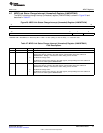
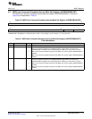
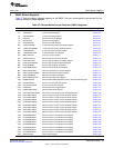
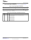
The MDIO user access register 1 (USERACCESS1) is shown in Figure 37 and described in Table 35.
Figure 37. MDIO User Access Register 1 (USERACCESS1)
31 30 29 28 26 25 21 20 16
GO WRITE ACK Reserved REGADR PHYADR
R/W1S-0 R/W-0 R/W-0 R-0 R/W-0 R/W-0
15 0
DATA
R/W-0
LEGEND: R/W = Read/Write; R = Read only; W1S = Write 1 to set (writing a 0 has no effect); -n = value after reset
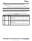
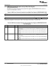
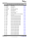
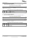
Table 35. MDIO User Access Register 1 (USERACCESS1) Field Descriptions
Bit Field Value Description
31 GO 0-1 Go bit. Writing 1 to this bit causes the MDIO state machine to perform an MDIO access when it is
convenient for it to do so; this is not an instantaneous process. Writing 0 to this bit has no effect.
This bit is writeable only if the MDIO state machine is enabled. This bit will self clear when the
requested access has been completed. Any writes to USERACCESS0 are blocked when the GO
bit is 1.
30 WRITE Write enable bit. Setting this bit to 1 causes the MDIO transaction to be a register write; otherwise,
it is a register read.
0 The user command is a read operation.
1 The user command is a write operation.
29 ACK 0-1 Acknowledge bit. This bit is set if the PHY acknowledged the read transaction.
28-26 Reserved 0 Reserved
25-21 REGADR 0-1Fh Register address bits. This field specifies the PHY register to be accessed for this transaction
20-16 PHYADR 0-1Fh PHY address bits. This field specifies the PHY to be accessed for this transaction.
15-0 DATA 0-FFFFh User data bits. These bits specify the data value read from or to be written to the specified PHY
register.
81
SPRUFL5B–April 2011 EMAC/MDIO Module
Submit Documentation Feedback
© 2011, Texas Instruments Incorporated