


Chapter 3 Hardware
LittleBoard 550 Reference Manual 25
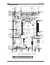
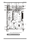
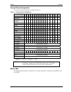
PC/104-Plus Interface (J21)
The PC/104-Plus uses a 120-pin (30x4) header interface. This interface header carries all of the
appropriate PCI signals operating at clock speeds up to 33MHz. The Northbridge, VT8606, integrates a
PCI arbiter that supports up to four devices with three external PCI masters. This interface header
accepts stackable modules and is located on the top of the board.
Table 3-4 provides the signals and descriptions for the PC/104-Plus bus pin-outs.
NOTE To conform to the PC/104-Plus standard, a key has been inserted
into a specific pin in the PC/104-Plus connector (A1).
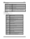
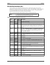
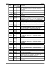
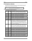
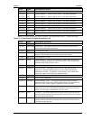
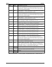
Table 3-4. PC/104-Plus Pin/Signal Descriptions (J21)
Pin # Signal Input/
Output
Description
1 (A1) Key Key pin (Not connected)
2 (A2) VI/O +5 volts ±5% power supply
3 (A3) AD05
T/S
PCI Address and Data Bus Line 5 – There are 32 signal lines
(address and data) and the signals on these lines are multiplexed. A
bus transaction consists of an address followed by one or more data
cycles.
4 (A4) C/BE0*
T/S
PCI Bus Command/Byte Enable 0 – This signal line is one of four
signal lines. These signal lines are multiplexed, so that during the
address cycle, the command is defined and during the data cycle,
the byte enable is defined.
5 (A5) GND Ground
6 (A6) AD11
T/S
PCI Address and Data Bus Line 11 – Refer to Pin 3 for more
information.
7 (A7) AD14
T/S
PCI Address and Data Bus Line 14 – Refer to Pin 3 for more
information.
8 (A8) +3.3V +3.3 volts ±5% power supply
9 (A9) SERR*
O/D
System Error – This signal is for reporting address parity errors.
10 (A10) GND Ground
11 (A11) STOP*
S/T/S
Stop – This signal indicates the current selected device is
requesting the master to stop the current transaction
12 (A12) +3.3V +3.3 volts ±5% power supply
13 (A13) FRAME*
S/T/S
PCI bus Frame access – This signal is driven by the current master
to indicate the start of a transaction and will remain active until the
final data cycle
14 (A14) GND Ground
15 (A15) AD18
T/S
PCI Address and Data Bus Line 18 – Refer to Pin 3 for more
information.
16 (A16) AD21
T/S
PCI Address and Data Bus Line 21 – Refer to Pin 3 for more
information.
17 (A17) +3.3V +3.3 volts ±5% power supply