


Chapter 3 Hardware
36 Reference Manual LittleBoard 550
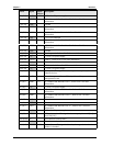
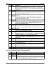
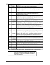
Pin # Signal Description
21 PDREQ Primary DMA Request – Used for DMA transfers between host and drive
(direction of transfer controlled by PDIOR* and PDIOW*). Also used in an
asynchronous mode with PDACK*. Drive asserts PDREQ when ready to transfer
or receive data.
22 GND Ground
23 PDIOW* Primary I/O Write Strobe – Strobe signal for write functions. Negative edge
enables data from a register or data port of the drive onto the host data bus.
Positive edge latches data at the host.
24 GND Ground
25 PDIOR*
Primary I/O Read Strobe – Strobe signal for read functions. Negative edge
enables data from a register or data port of the drive onto the host data bus.
Positive edge latches data at the host.
26 GND Ground
27 PDIORDY Primary I/O Channel Ready – When negated extends the host transfer cycle of any
host register access when the drive is not ready to respond to a data transfer
request. High impedance if asserted.
28 NU Not used (Pull down to ground through 470 ohm resistor)
29 PDACK*
Primary DMA Acknowledge – Used by the host to acknowledge data has been
accepted or data is available. Used in response to PDREQ asserted.
30 GND Ground
31 IRQ14
Interrupt Request 14 – Asserted by drive when it has pending interrupt (PIO
transfer of data to or from the drive to the host).
32 NC Not connected
33 PDA1
Primary Disk Address 1 – One of three signals (0 – 2) used to indicate which byte
in the ATA command block or control block is being accessed.
34 PD33_66 UDMA 33/66 Sense – Used to detect the presence of an 80 conductor IDE cable
on the primary IDE channel. Enables BIOS to sense which DMA mode to use for
IDE devices.
35 PDA0 Primary Disk Address 0 – Refer to PDA1 on pin-33 for more information.
36 PDA2 Primary Disk Address 2 – Refer to PDA1 on pin-33 for more information.
37 PDCS1# Primary Slave/Master Chip Select 1 – Used to select the host-accessible
Command Block Register.
38 PDCS3# Primary Slave/Master Chip Select 3 – Used to select the host-accessible
Command Block Register.
39 IDEPACT Connected through 10k ohm resistor to +5V
40 GND Ground
Notes: The shaded area denotes power or ground. The signals marked with * = Negative true logic.
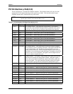
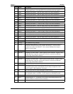
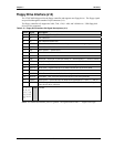
Table 3-10. Secondary IDE Interface Pin/Signal Descriptions (J17)
Pin # Signal Description
1 IDERST* IDE Reset – Low active hardware reset (RSTDRV inverted)
2 GND Ground
3SDD7
Secondary Disk Data 7 – These signals (D0-D15) carry the Data, Commands,
and Status between the host and the controller. D0 is the LSB of the even Byte
of the Word. D8 is the LSB of the Odd Byte of the Word.