


Chapter 3 Hardware
LittleBoard 550 Reference Manual 31
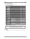
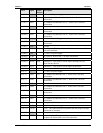
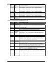
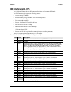
Pin # Signal Description (J1 Row A)
23 (A23) SA8 System Address 8 – Refer to SA19, pin-A12, for more information.
24 (A24) SA7 System Address 7 – Refer to SA19, pin-A12, for more information.
25 (A25) SA6 System Address 6 – Refer to SA19, pin-A12, for more information.
26 (A26) SA5 System Address 5 – Refer to SA19, pin-A12, for more information.
27 (A27) SA4 System Address 4 – Refer to SA19, pin-A12, for more information.
28 (A28) SA3 System Address 3 – Refer to SA19, pin-A12, for more information.
29 (A29) SA2 System Address 2 – Refer to SA19, pin-A12, for more information.
30 (A30) SA1 System Address 1 – Refer to SA19, pin-A12, for more information.
31 (A31) SA0 System Address 0 – Refer to SA19, pin-A12, for more information.
32 (A32) GND Ground
Notes: The shaded area denotes power or ground. The signals marked with * = Negative true logic.
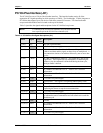
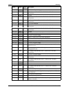
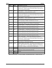
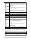
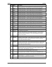
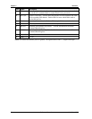
Table 3-6. PC/104 Interface Pin/Signal Descriptions (J1B)
Pin # Signal Descriptions (J1 Row B)
33 (B1) GND Ground
34 (B2) RESETDRV Reset Drive – This signal is used to reset or initialize system logic on
power up or subsequent system reset.
35 (B3) +5V +5 volt power ±10%
36 (B4) IRQ9 Interrupt request 9 – Asserted by a device when it has pending interrupt
request. Only one device may use the request line at a time.
37 (B5) -5V Not connected (-5 volts)
38 (B6) DRQ2 DMA Request 2 – Used by I/O resources to request DMA service, or to
request ownership of the bus as a bus master device. Must be held high
until associated DACK2 line is active.
39 (B7) -12V Not connected (-12 volts)
40 (B8) ENDXFR*
Zero Wait State – This signal is driven low by a bus slave device to
indicate it is capable of performing a bus cycle without inserting any
additional wait states. To perform a 16-bit memory cycle without wait
states, this signal is derived from an address decode.
41 (B9) +12V +12 Volts
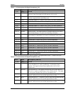
42 (B10) Key Key Pin (Not connected)
43 (B11) SMEMW* System Memory Write – This signal is used by bus owner to request a
memory device to store data currently on the data bus and only active for
the lower 1MB. Used for legacy compatibility with 8-bit cards.
44 (B12) SMEMR* System Memory Read – This signal is used by bus owner to request a
memory device to drive data onto the data bus and only active for lower
1MB. Used for legacy compatibility with 8-bit cards.
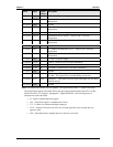
45 (B13) IOW* I/O Write – This strobe signal is driven by the owner of the bus (ISA bus
master or DMA controller) and instructs the selected I/O device to capture
the write data on the data bus.
46 (B14) IOR* I/O Read – This strobe signal is driven by the owner of the bus (ISA bus
master or DMA controller) and instructs the selected I/O device to drive
read data onto the data bus.