


Chapter 3 Hardware
30 Reference Manual LittleBoard 550
PC/104 Interface (J1A,B,C,D)
The PC/104 Bus uses a 104-pin 100 mil header interface. This interface header will carry all of the
appropriate PC/104 signals operating at clock speeds up to 8MHz. This interface header accepts
stackable modules and is located on the top of the board.
NOTE To conform to the PC/104 standard, keys have been inserted into
specific pins in the PC/104 connector (B10, C19).
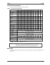
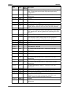
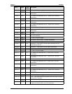
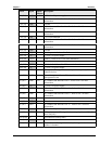
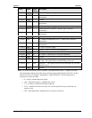
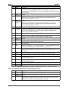
Table 3-5. PC/104 Interface Pin/Signal Descriptions (J1A)
Pin # Signal Description (J1 Row A)
1 (A1) IOCHCHK*
I/O Channel Check – This signal may be activated by ISA boards to
request that a non-maskable interrupt (NMI) be generated to the system
processor. It is driven active to indicate uncorrectable error detection.
2 (A2) SD7 System Data 7 – This signal (0 to 19) provides a system data bit.
3 (A3) SD6 System Data 6 – Refer to SD7, pin-A2, for more information.
4 (A4) SD5 System Data 5 – Refer to SD7, pin-A2, for more information.
5 (A5) SD4 System Data 4 – Refer to SD7, pin-A2, for more information.
6 (A6) SD3 System Data 3 – Refer to SD7, pin-A2, for more information.
7 (A7) SD2 System Data 2 – Refer to SD7, pin-A2, for more information.
8 (A8) SD1 System Data 1 – Refer to SD7, pin-A2, for more information.
9 (A9) SD0 System Data 0 – Refer to SD7, pin-A2, for more information.
10 (A10) IOCHRDY
I/O Channel Ready – This signal allows slower ISA boards to lengthen
I/O or memory cycles by inserting wait states. This signal’s normal state
is active high (ready). ISA boards drive the signal inactive low (not
ready) to insert wait states. Devices using this signal to insert wait states
should drive it low immediately after detecting a valid address decode and
an active read, or write command. The signal is released high when the
device is ready to complete the cycle.
11 (A11) AEN Address Enable – This signal is used to degate the system processor and
other devices from the bus during DMA transfers. When this signal is
active, the system DMA controller has control of the address, data, and
read/write signals. This signal should be included as part of ISA board
select decodes to prevent incorrect board selects during DMA cycles.
12 (A12) SA19 System Address 19 – This signal (0 to 19) provides a system address bit.
13 (A13) SA18 System Address 18 – Refer to SA19, pin-A12, for more information.
14 (A14) SA17 System Address 17 – Refer to SA19, pin-A12, for more information.
15 (A15) SA16 System Address 16 – Refer to SA19, pin-A12, for more information.
16 (A16) SA15 System Address 15 – Refer to SA19, pin-A12, for more information.
17 (A17) SA14 System Address 14 – Refer to SA19, pin-A12, for more information.
18 (A18) SA13 System Address 13 – Refer to SA19, pin-A12, for more information.
19 (A19) SA12 System Address 12– Refer to SA19, pin-A12, for more information.
20 (A20) SA11 System Address 11 – Refer to SA19, pin-A12, for more information.
21 (A21) SA10 System Address 10 – Refer to SA19, pin-A12, for more information.
22 (A22) SA9 System Address 9 – Refer to SA19, pin-A12, for more information.