


Chapter 3 Hardware
LittleBoard 550 Reference Manual 33
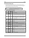
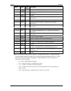
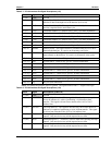
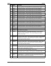
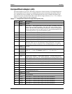
Table 3-7. PC/104 Interface Pin/Signal Descriptions (J1C)
Pin # Signal Descriptions (J1 Row C)
1 (C0) GND Ground
2 (C1) SBHE* System Byte High Enable – This signal is driven low to indicate a
transfer of data on the high half of the data bus (D15 to D8).
3 (C2) LA23
Lactchable Address 23 – This signal must be latched by the resource if
the line is required for the entire data cycle.
4 (C3) LA22 Lactchable Address 22 – Refer to LA23, pin-C2, for more information.
5 (C4) LA21 Lactchable Address 21 – Refer to LA23, pin-C2, for more information.
6 (C5) LA20 Lactchable Address 20 – Refer to LA23, pin-C2, for more information.
7 (C6) LA19 Lactchable Address 19 – Refer to LA23, pin-C2, for more information.
8 (C7) LA18 Lactchable Address 18 – Refer to LA23, pin-C2, for more information.
9 (C8) LA17 Lactchable Address 17 – Refer to LA23, pin-C2, for more information.
10 (C9) MEMR* Memory Read – This signal instructs a selected memory device to drive
data onto the data bus. It is active on all memory read cycles.
11 (C10) MEMW* Memory Write – This signal instructs a selected memory device to store
data currently on the data bus. It is active on all memory write cycles.
12 (C11) SD8 System Data 8 – Refer to SD7, pin-A2, for more information.
13 (C12) SD9 System Data 9 – Refer to SD7, pin-A2, for more information.
14 (C13) SD10 System Data 10 – Refer to SD7, pin-A2, for more information.
15 (C14) SD11 System Data 11 – Refer to SD7, pin-A2, for more information.
16 (C15) SD12 System Data 12 – Refer to SD7, pin-A2, for more information.
17 (C16) SD13 System Data 13 – Refer to SD7, pin-A2, for more information.
18 (C17) SD14 System Data 14 – Refer to SD7, pin-A2, for more information.
19 (C18) SD15 System Data 15 – Refer to SD7, pin-A2, for more information.
20 (C19) Key Key Pin (Not connected)
Notes: The shaded area denotes power or ground. The signals marked with * = Negative true logic.
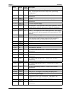
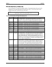
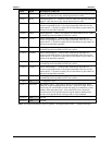
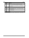
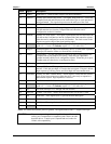
Table 3-8. PC/104 Interface Pin/Signal Descriptions (J1D)
Pin # Signal Descriptions (J1 Row D)
21 (D0) GND Ground
22 (D1) MEMCS16* Memory Chip Select 16 – This is signal is driven low by a memory slave
device to indicates it is cable of performing a 16-bit memory data
transfer. This signal is driven from a decode of the LA23 to LA17
address lines.
23 (D2) IOCS16* I/O Chip Select 16 – This signal is driven low by an I/O slave device to
indicate it is capable of performing a 16-bit I/O data transfer. This signal
is driven from a decode of the SA15 to SA0 address lines.
24 (D3) IRQ10 Interrupt Request 10 – Asserted by a device when it has pending interrupt
request. Only one device may use the request line at a time.
25 (D4) IRQ11 Interrupt Request 11 – Asserted by a device when it has pending interrupt
request. Only one device may use the request line at a time.
26 (D5) IRQ12 Interrupt Request 12 – Asserted by a device when it has pending interrupt
request. Only one device may use the request line at a time.