


Chapter 3 Hardware
28 Reference Manual LittleBoard 550
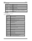
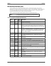
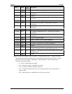
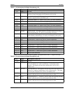
Pin # Signal Input/
Output
Description
74 (C14) +3.3V +3.3 volts ±5% power supply
75 (C15) AD17
T/S
PCI Address and Data Bus Line 17 – Refer to Pin 3 for more
information.
76 (C16) GND Ground
77 (C17) AD22
T/S
PCI Address and Data Bus Line 22 – Refer to Pin 3 for more
information.
78 (C18) IDSEL1
Initialization Device Select 1 – Refer to Pin 18 for more
information
79 (C19) VI/O
NC
(+5V) Not connected
80 (C20) AD25
T/S
PCI Address and Data Bus Line 25 – Refer to Pin 3 for more
information.
81 (C21) AD28
T/S
PCI Address and Data Bus Line 28 – Refer to Pin 3 for more
information.
82 (C22) GND Ground
83 (C23) REQ1*
T/S
Bus Request 1 – Refer to Pin 23 for more information.
84 (C24) +5V +5 volts ±5% power supply
85 (C25) GNT2*
T/S
Grant 2 – Refer to Pin 25 for more information
86 (C26) GND Ground
87 (C27) CLK3
In
PCI clock 3 – Refer to Pin 27 for more information
88 (C28) +5V +5 volts ±5% power supply
89 (C29) INTB*
O/D
Interrupt B – This signal is used to request interrupts only for multi-
function devices.
90 (C30) PME* Power Management Event – This signal is used for power
management events
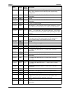
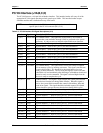
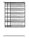
91 (D1) AD00
T/S
PCI Address and Data Bus Line 0 – Refer to Pin 3 for more
information.
92 (D2) +5V +5 volts ±5% power supply
93 (D3) AD03
T/S
PCI Address and Data Bus Lines 3 – Refer to Pin 3 for more
information.
94 (D4) AD06
T/S
PCI Address and Data Bus Lines 6 – Refer to Pin 3 for more
information.
95 (D5) GND Ground
96 (D6) GND Ground
97 (D7) AD12
T/S
PCI Address and Data Bus Line 12 – Refer to Pin 3 for more
information.
98 (D8) +3.3V +3.3 volts ±5% power supply
99 (D9) PAR
T/S
PCI bus Parity bit – This signal is the even parity bit on AD[31:0]
and C/BE[3:0]*
100 (D10) NC
NC
Not connected (Snoop Done)
101 (D11) GND Ground
102 (D12) Devsel*
S/T/S
Device Select – This signal is driven by the target device when its
address is decoded.