


Chapter 3 Hardware
LittleBoard 550 Reference Manual 39
CompactFlash Adapter (J23)
The board contains a Type II PC card socket, which allows for the insertion of a CompactFlash Card.
The CompactFlash (CF) Card acts as a standard IDE Drive and is connected to the primary IDE bus.
If a CompactFlash card is installed, only one additional IDE drive may be added to the primary bus.
Jumpers are used to select the Master/Slave mode and the voltage selection (+5V or +3.3V). Refer to
Table 2-4, Jumper Settings for more information.
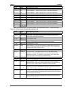
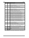
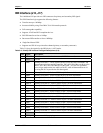
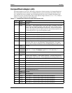
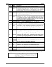
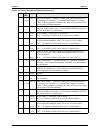
Table 3-11. CompactFlash Interface Pin/Signal Descriptions (J23)
Pin # Signal Description
1 GND Ground
2 PDD3 Disk Data 3 – These signals (D0-D15) carry the Data, Commands, and Status
between the host and the controller. D0 is the LSB of the even Byte of the
Word. D8 is the LSB of the Odd Byte of the Word. All Task File operations
occur in byte mode on the low order bus D0-D7, while all data transfers are
16 bit using D0-D15 to provide the disk data signals.
3 PDD4 Disk Data 4 – Refer to PDD3 on pin-2 for more information.
4 PDD5 Disk Data 5 – Refer to PDD3 on pin-2 for more information.
5 PDD6 Disk Data 6 – Refer to PDD3 on pin-2 for more information.
6 PDD7 Disk Data 7 – Refer to PDD3 on pin-2 for more information.
7PDCE1*
Primary Chip Select 1 – This signal, along with CE2*, selects the card and
indicates when a byte or word operation is being performed. This signal
accesses the even byte or odd byte of the word depending on A0 and CE2*.
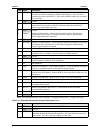
8, 9, 10,
11, 12
GND Ground
13 VCC CF power – This voltage is determined by setting of JP3, CF Voltage Select
(pins 1-2 = +5 volts ±5% Default, or pins 2-3 = +3.3 volts ±5%)
14, 15,
16, 17
GND Ground
18 PDA2
Primary Disk Address 2 – One of three signals (0 – 2) used to select one of
eight registers in the Task File. The host grounds all remaining address lines.
19 PDA1 Primary Disk Address 1 – Refer to A2 on pin-18 for more information.
20 PDA0 Primary Disk Address 0 – Refer to A2 on pin-18 for more information.
21 PDD0 Primary Disk Data 0 – Refer to PDD3 on pin-2 for more information.
22 PDD1 Primary Disk Data 1 – Refer to PDD3 on pin-2 for more information.
23 PDD2 Primary Disk Data 2 – Refer to PDD3 on pin-2 for more information.
24 NC Not connected (IOCS16*)
25 GND Ground
26 NC Not connected
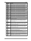
27 PDD11 Disk Data 11 – Refer to PDD3 on pin-2 for more information.
28 PDD12 Disk Data 12 – Refer to PDD3 on pin-2 for more information.
29 PDD13 Disk Data 13 – Refer to PDD3 on pin-2 for more information.
30 PDD14 Disk Data 14 – Refer to PDD3 on pin-2 for more information.