


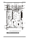


Chapter 3 Hardware
26 Reference Manual LittleBoard 550
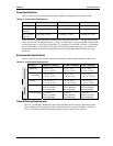
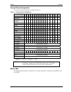
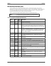
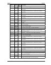
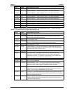
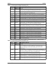
Pin # Signal Input/
Output
Description
18 (A18) IDSEL0
In
Initialization Device Select 0 – This signal line is one of four signal
lines. These signals are used as the chip-select signals during
configuration
19 (A19) AD24
T/S
PCI Address and Data Bus Line 24 – Refer to Pin 3 for more
information.
20 (A20) GND Ground
21 (A21) AD29
T/S
PCI Address and Data Bus Line 29 – Refer to Pin 3 for more
information.
22 (A22) +5V +5 volts ±5% power supply
23 (A23) REQ0*
T/S
Bus Request 0 – This signal line is one of three signal lines. These
signals indicate the device desires use of the bus to the arbitrator.
24 (A24) GND Ground
25 (A25) GNT1*
T/S
Grant 1 – This signal line is one of three signal lines. These signal
lines indicate access has been granted to the requesting device (PCI
Masters).
26 (A26) +5V +5 volts ±5% power supply
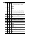
27 (A27) CLK2 In PCI clock 2 – This signal line is one of four signal lines. These
clock signals provide the timing outputs for four external PCI
devices and the timing for all transactions on the PCI bus
28 (A28) GND Ground
29 (A29) +12V +12 volts ±5% power supply
30 (A30) NC Not connected - Reserved
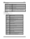
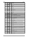
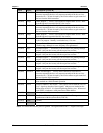
31 (B1) NC Not connected - Reserved
32 (B2) AD02
T/S
PCI Address and Data Bus Line 2 – Refer to Pin 3 for more
information.
33 (B3) GND Ground
34 (B4) AD07
T/S
PCI Address and Data Bus Line 7 – Refer to Pin 3 for more
information.
35 (B5) AD09
T/S
PCI Address and Data Bus Line 9 – Refer to Pin 3 for more
information.
36 (B6) VI/O +5 volts ±5% power supply
37 (B7) AD13
T/S
PCI Address and Data Bus Lines 13 – Refer to Pin 3 for more
information.
38 (B8) C/BE1*
T/S
PCI Bus Command/Byte Enable 1 – Refer to Pin 4 for more
information.
39 (B9) GND Ground
40 (B10) PERR* Parity Error – This signal is for reporting data parity errors.
41 (B11) +3.3V +3.3 volts ±5% power supply
42 (B12) TRDY*
S/T/S
Target Ready – This signal indicates the selected device’s ability to
complete the current cycle of transaction. Both IRDY* and
TRDY* must be asserted to terminate a data cycle
43 (B13) GND Ground
44 (B14) AD16
T/S
PCI Address and Data Bus Line 16 – Refer to Pin 3 for more
information.