


Chapter 3 Hardware
58 Reference Manual LittleBoard 550
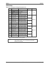
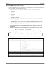
LVDS Interface
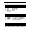
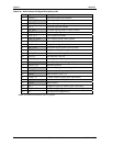
Table 3-26. LVDS Interface Pin/Signal Descriptions (J31)
Pin # Signal Description Line Channel
1 3.3V_Panel +3.3V source
2 5V_Panel +5V source
3 GND Ground
4 GND Ground
NA NA
5 LVDS_Y0M Data Negative Output
6 LVDS_Y0P Data Positive Output
0
7 LVDS_Y1M Data Negative Output
8 LVDS_Y1P Data Positive Output
1
9 LVDS_Y2M Data Negative Output
10 LVDS_Y2P Data Positive Output
2
11 LVDS_CLKYM Clock Negative Output
12 LVDS_CLKYP Clock Positive Output
Clock
Channel 1
13 LVDS_Z0M Data Negative Output
14 LVDS_Z0P Data Positive Output
0
15 LVDS_Z1M Data Negative Output
16 LVDS_Z1P Data Positive Output
1
17 LVDS_Z2M Data Negative Output
18 LVDS_Z2P Data Positive Output
2
19 LVDS_CLKZM Clock Negative Output
20 LVDS_CLKZP Clock Positive Output
Clock
Channel 2
Notes: The shaded area denotes power or ground.
NOTE Pins 5-12 constitute 1
st
channel interface of two channels, or a
single channel interface. Pins 13-20 constitute 2nd channel
interface of two channels.