292 Software Developer’s Manual
Register Descriptions
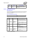
13.4.16 Packet Buffer Allocation
PBA (01000H; R/W)
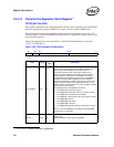
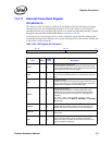
This register sets the on-chip receive and transmit storage allocation ratio. The receive allocation
value is read/write for the lower seven bits. The receive allocation value must be a multiple of eight
(multiple of two for the
82547GI/EI B1 stepping). The transmit allocation is read-only and is
calculated based on PBA.RXA.
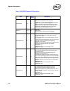
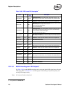
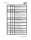
Table 13-62. PBA Register Bit Description
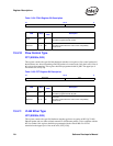
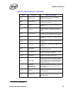
1111b GND/LED_OFF
Always low. Assuming no optional inversion
selected, causes output pin low / LED OFF for
typical LED circuit.
Mode Pneumonic State / Event Indicated
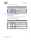
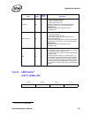
31 16 15 0
TXA RXA
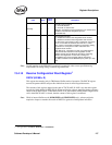
Field Bit(s) Initial Value Description
RXA
6:0
15:0 (82541xx
and 82547GI/EI)
0030h
1
0016h (82547EI A0-B0
steppings)
001Eh (82547GI B1
stepping)
Receive Packet Buffer Allocation in KB
Sets the size of the receive packet buffer.
The value of this field must be a multiple of eight.
The upper nine bits are read only as 0b. Default is
48 KB.
For the 82541xx and 82547GI/EI, the upper unused
bits are read only as 0b. The default is 48 KB for the
82541xx, 24 KB for the 82547EI, and 20 KB for the
82547GI.
RXA_R
2
15:7 0b
Receive Packet Buffer Allocation – Upper Bits
Provides the upper nine bits of the receive packet
buffer allocation.
Read only bits - Read as 0b.
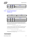
TXA
31:16
15:00 (82541xx
and 82547GI/EI)
0010h
0012h (82547EI A0-B0
steppings)
000Ah (82547GI B1
stepping)
Transmit Packet Buffer Allocation
Provides the size of the transmit packet buffer. The
value is in units of KB. These bits are read only.
TXA is calculated based on RXA value: TXA = 64 –
RXA.
For the 82547GI/EI, TXA is calculated based on
RXA value: TXA = 40 – RXA.
1. Not applicable to the 82547GI/EI.
2. Not applicable to the 82541xx or 82547GI/EI.


