Datasheet
9
Networkin
g
Silicon —GD82559ER
3.2.3 S
y
stem and Power Mana
g
ement Si
g
nals
3.3 Local Memor
y
Interface Si
g
nals
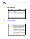
Symbol Type Name and Function
CLK IN
Clock.
The Clock si
g
nal provides the timin
g
for all PCI transactions
and is an input si
g
nal to ever
y
PCI device. The 82559ER re
q
uires a
PCI Clock si
g
nal
(
fre
q
uenc
y
g
reater than or e
q
ual to 16 MHz
)
for
nominal operation. The 82559ER supports Clock si
g
nal suspension
usin
g
the Clockrun protocol.
CLKRUN#
IN/OUT
O/D
Clockrun.
The Clockrun si
g
nal is used b
y
the s
y
stem to pause or slow
down the PCI Clock si
g
nal. It is used b
y
the 82559ER to enable or
disable suspension of the PCI Clock si
g
nal or restart of the PCI clock.
When the Clockrun si
g
nal is not used, this pin should be connected to
an external pull-down resistor.
RST# IN
Reset.
The PCI Reset si
g
nal is used to place PCI re
g
isters,
se
q
uencers, and si
g
nals into a consistent state. When RST# is
asserted, all PCI output si
g
nals will be tri-stated.
PME# O/D
Power Management Event.
The Power Mana
g
ement Event si
g
nal
indicates that a power mana
g
ement event has occurred in a PCI bus
s
y
stem.
ISOLATE# IN
Isolate.
The Isolate si
g
nal is used to isolate the 82559ER from the
PCI bus. When Isolate is active
(
low
)
, the 82559ER does not drive its
PCI outputs
(
except PME#
)
or sample its PCI inputs
(
includin
g
CLK
and RST#
)
. If the 82559ER is not powered b
y
an auxiliar
y
power
source, the ISOLATE# pin should be pulled hi
g
h to the bus Vcc
throu
g
h a 4.7K-62K resistor.
ALTRST# IN
Alternate Reset.
The Alternate Reset si
g
nal is used to reset the
82559ER on power-up. In s
y
stems that support an auxiliar
y
power
suppl
y
, ALTRST# should be connected to a power-up detection circuit.
Otherwise, ALTRST# should be tied to V
cc
.
VIO
B
IN
Voltage Input/Output.
The VIO pin is the a volta
g
e bias pin for the
PCI interface. This pin should be connected to 5V ± 5% in a 5 volt PCI
s
y
stem and 3.3 volts in a 3.3 volt PCI s
y
stem. Be sure to install a 10K
pull-up resistor. This resistor acts as a current limit resistor in s
y
stem
where the VIO bias volta
g
e ma
y
be shutdown. In this cases the
82559ER ma
y
consume additional current without a resistor.
Symbol Type Name and Function
FLD[7:0] T/S
Flash Data Input/Output.
These pins are used for Flash data
interface.
FLA[16]/
CLK25
OUT
Flash Address[16]/25 MHz Clock.
This multiplexed pin is controlled
b
y
the status of the Flash Address[7]
(
FLA[7]
)
pin. If FLA[7] is left
floatin
g
, this pin is used as FLA[16]; otherwise, if FLA[7] is connected
to a pull-up resistor, this pin is used as a 25 MHz clock.
FLA[15]/
EESK
OUT
Flash Address[15]/EEPROM Data Output.
Durin
g
Flash accesses,
this multiplexed pin acts as the Flash Address [15] output si
g
nal.
Durin
g
EEPROM accesses, it acts as the serial shift clock output to
the EEPROM.
FLA[14]/
EEDO
IN/OUT
Flash Address[14]/EEPROM Data Output.
Durin
g
Flash accesses,
this multiplexed pin acts as the Flash Address [14] output si
g
nal.
Durin
g
EEPROM accesses, it acts as serial input data to the EEPROM
Data Output si
g
nal.


