


Datasheet
iii
Networking Silicon — GD82559ER
Contents
1. INTRODUCTION.............................................................................................................................1
1.1 GD82559ER Overview .......................................................................................................1
1.2 Suggested Reading ............................................................................................................1
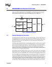
2. GD82559ER ARCHITECTURAL OVERVIEW ................................................................................3
2.1 Parallel Subsystem Overview.............................................................................................3
2.2 FIFO Subsystem Overview.................................................................................................4
2.3 10/100 Mbps Serial CSMA/CD Unit Overview....................................................................5
2.4 10/100 Mbps Physical Layer Unit .......................................................................................5
3. SIGNAL DESCRIPTIONS...............................................................................................................7
3.1 Signal Type Definitions.......................................................................................................7
3.2 PCI Bus Interface Signals...................................................................................................7
3.2.1 Address and Data Signals..................................................................................7
3.2.2 Interface Control Signals ....................................................................................8
3.2.3 System and Power Management Signals...........................................................9
3.3 Local Memory Interface Signals .........................................................................................9
3.4 Testability Port Signals .....................................................................................................10
3.5 PHY Signals .....................................................................................................................11
4. GD82559ER MEDIA ACCESS CONTROL FUNCTIONAL DESCRIPTION.................................13
4.1 82559ER Initialization.......................................................................................................13
4.1.1 Initialization Effects on 82559ER Units ............................................................13
4.2 PCI Interface.....................................................................................................................14
4.2.1 82559ER Bus Operations.................................................................................14
4.2.2 Clockrun Signal ................................................................................................22
4.2.3 Power Management Event Signal ....................................................................22
4.2.4 Power States ....................................................................................................23
4.2.5 Wake-up Events ...............................................................................................27
4.3 Parallel Flash Interface.....................................................................................................28
4.4 Serial EEPROM Interface.................................................................................................28
4.5 10/100 Mbps CSMA/CD Unit............................................................................................30
4.5.1 Full Duplex .......................................................................................................31
4.5.2 Flow Control .....................................................................................................31
4.5.3 Address Filtering Modifications.........................................................................31
4.5.4 Long Frame Reception.....................................................................................31
4.6 Media Independent Interface (MII) Management Interface...............................................32
5. GD82559ER TEST PORT FUNCTIONALITY ...............................................................................33
5.1 Introduction.......................................................................................................................33
5.2 Asynchronous Test Mode.................................................................................................33
5.3 Test Function Description.................................................................................................33
5.4 85/85.................................................................................................................................33
5.5 TriState .............................................................................................................................34
5.6 Nand - Tree ......................................................................................................................34
6. GD82559ER PHYSICAL LAYER FUNCTIONAL DESCRIPTION................................................37
6.1 100BASE-TX PHY Unit ....................................................................................................37
6.1.1 100BASE-TX Transmit Clock Generation ........................................................37