


GD82559ER — Networkin
g
Silicon
48
Datasheet
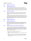
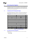
7.1.2 PCI Command Re
g
ister
The 82559ER Command register at word address 04h in the PCI configuration space provides
control over the 82559ER’s ability to generate and respond to PCI cycles
.
If a 0His written to this
register, the 82559ER is logically disconnected from the PCI bus for all accesses except
configuration accesses
.
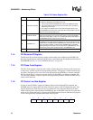
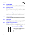
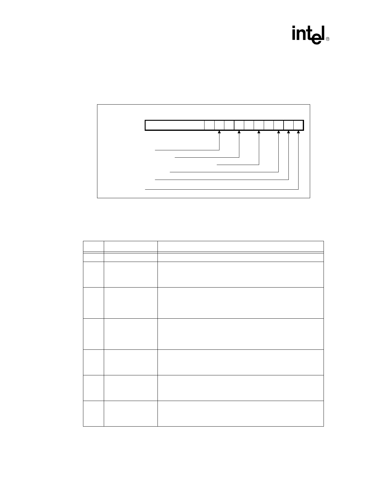
The format of this register is shown in the figure below.
Note that bits three, five, seven, and nine are set to 0b. The table below describes the bits of the PCI
Command register.
Fi
g
ure 18. PCI Command Re
g
ister
Reserved
SERR# Enable
Parity Error Response
Memory Write and Invalidate Enable
Bus Master Enable
Memory Space
IO space
0000
1015 01234567
89
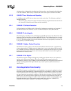
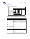
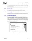
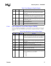
Table 5. PCI Command Re
g
ister Bits
Bits Name Description
15:10 Reserved These bits are reserved and should be set to 000000b.
8 SERR# Enable
This bit controls a device’s abilit
y
to enable the SERR# driver. A value of 0b
disables the SERR# driver. A value of 1b enables the SERR# driver. This
bit must be set to report address parit
y
errors. In the 82559ER, this bit is
confi
g
urable and has a default value of 0b.
6 Parit
y
Error Control
This bit controls a device’s response to parit
y
errors. A value of 0b causes
the device to i
g
nore an
y
parit
y
errors that it detects and continue normal
operation. A value of 1b causes the device to take normal action when a
parit
y
error is detected. This bit must be set to 0b after RST# is asserted. In
the 82559ER, this bit is confi
g
urable and has a default value of 0b.
4
Memor
y
Write and
Invalidate Enable
This bit controls a device’s abilit
y
to use the Memor
y
Write and Invalidate
command. A value of 0b disables the device from usin
g
the Memor
y
Write
and Invalidate Enable command. A value of 1b enables the device to use
the Memor
y
Write and Invalidate command. In the 82559ER, this bit is
confi
g
urable and has a default value of 0b.
2 Bus Master
This bit controls a device’s abilit
y
to act as a master on the PCI bus. A
value of 0b disables the device from
g
eneratin
g
PCI accesses. A value of
1b allows the device to behave as a bus master. In the 82559ER, this bit is
confi
g
urable and has a default value of 0b.
1 Memor
y
Space
This bit controls a device’s response to the memor
y
space accesses. A
value of 0b disables the device response. A value of 1b allows the device
to respond to memor
y
space accesses. In the 82559ER, this bit is
confi
g
urable and its default value of 0b.
0 I/O Space
This bit controls a device’s response to the I/O space accesses
.
A value of
0b disables the device response. A value of 1b allows the device to
respond to I/O space accesses. In the 82559ER, this bit is confi
g
urable and
the default value of 0b.