Datasheet
37
Networkin
Silicon — GD82559ER
6. GD82559ER Ph
sical La
er Functional Descri
tion
6.1 100BASE-TX PHY Unit
6.1.1 100BASE-TX Transmit Clock Generation
A 25 MHz crystal or a 25 MHz oscillator is used to drive the PHY unit’s X1 and X2 pins. The PHY
unit derives its internal transmit digital clocks from this crystal or oscillator input. The internal
Transmit Clock signal is a derivative of the 25 MHz internal clock. The accuracy of the external
crystal or oscillator must be ± 0.0005% (50 PPM).
6.1.2 100BASE-TX Transmit Blocks
The transmit subsection of the PHY unit accepts nibble-wide data from the CSMA/CD unit. The
transmit subsection passes data unconditionally to the 4B/5B encoder.
The 4B/5B encoder accepts nibble-wide data (4 bits) from the CSMA unit and compiles it into 5-
bit-wide parallel symbols. These symbols are scrambled and serialized into a 125 Mbps bit stream,
converted by the analog transmit driver into a MLT-3 waveform format, and transmitted onto the
Unshielded Twisted Pair (UTP) or Shielded Twisted Pair (STP) wire.
6.1.2.1 100BASE-TX 4B/5B Encoder
The 4B/5B encoder complies with the IEEE 802.3u 100BASE-TX standard. Four bits are encoded
according to the transmit 4B/5B lookup table. The lookup table matches a 5-bit code to each 4-bit
code.
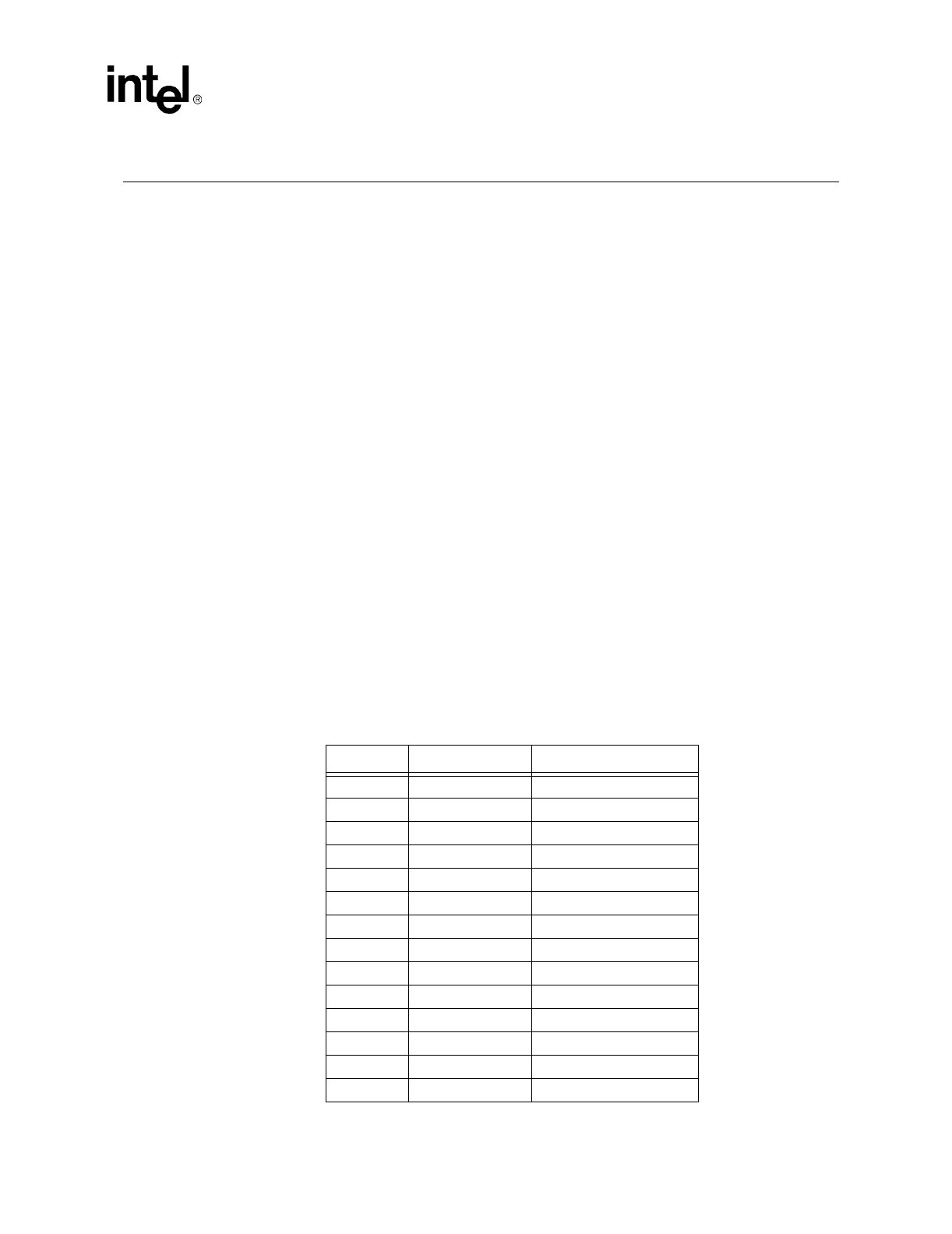
The table below illustrates the 4B/5B encoding scheme associated with the given symbol.
Table 3. 4B/5B Encoder
Symbol 5B Symbol Code 4B Nibble Code
0 11110 0000
1 01001 0001
2 10100 0010
3 10101 0011
4 01010 0100
5 01011 0101
6 01110 0110
7 01111 0111
8 10010 1000
9 10011 1001
A 10110 1010
B 10111 1011
C 11010 1100
D 11011 1101


