


Datasheet
51
Networkin
g
Silicon — GD82559ER
Note:
Bit 3 is set to 1b only if the value 00001000b (8H) is written to this register, and bit 4 is set to 1b
only if the value of 00010000b (16H) is written to this register. All other bits are read only and will
return a value of 0b on read.
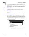
This register is expected to be written by the BIOS and the 82559ER driver should not write to it.
7.1.7 PCI Latenc
y
Timer
The Latency Timer register is a byte wide register. When the 82559ER is acting as a bus master,
this register defines the amount of time, in PCI clock cycles, that it may own the bus.
7.1.8 PCI Header T
yp
e
The Header Type register is a byte read only register. It is hard-coded to equal to 00h for a single
function card.
7.1.9 PCI Base Address Re
g
isters
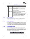
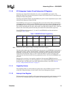
One of the most important functions for enabling superior configurability and ease of use is the
ability to relocate PCI devices in address spaces. The 82559ER contains three types of Base
Address Registers (BARs). Two are used for memory mapped resources, and one is used for I/O
mapping. Each register is 32 bits wide. The least significant bit in the BAR determines whether it
represents a memory or I/O space. The figures below show the layout of a BAR for both memory
and I/O mapping. After determining this information, power-up software can map the memory and
I/O controllers into available locations and proceed with system boot. To do this mapping in a
device independent manner, the base registers for this mapping are placed in the predefined header
portion of configuration space. Device drivers can then access this configuration space to
determine the mapping of a particular device.
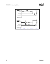
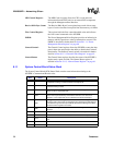
Fi
g
ure 21. Base Address Re
g
ister for Memor
y
Ma
pp
in
g
Base Address 0
0
31
4321
Prefetchable
Set to 0b in 82559ER
T
y
pe
00 - locate an
y
where in 32-bit address space
01 - locate below 1 Mb
y
te
10 - locate an
y
where in 64-bit address space
11 - reserved
Memor
y
space indicator