


Datasheet
19
Networkin
g
Silicon — GD82559ER
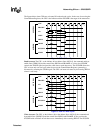
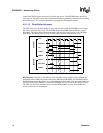
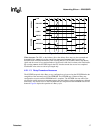
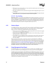
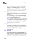
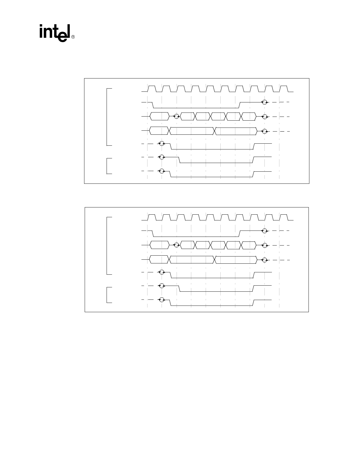
8 depict memory read and write burst cycles. For bus master cycles, the 82559ER is the initiator
and the host main memory (or the PCI host bridge, depending on the configuration of the system) is
the target.
The CPU provides the 82559ER with action commands and pointers to the data buffers that reside
in host main memory. The 82559ER independently manages these structures and initiates burst
memory cycles to transfer data to and from them. The 82559ER uses the Memory Read Multiple
(MR Multiple) command for burst accesses to data buffers and the Memory Read Line (MR Line)
command for burst accesses to control structures. For all write accesses to the control structure, the
82559ER uses the Memory Write (MW) command. For write accesses to data structure, the
82559ER may use either the Memory Write or Memory Write and Invalidate (MWI) commands.
Read Accesses:
The 82559ER performs block transfers from host system memory to perform
frame transmission on the serial link. In this case, the 82559ER initiates zero wait state
memory
read burst cycles for these accesses. The length of a burst is bounded by the system and the
82559ER’s internal FIFO. The length of a read burst may also be bounded by the value of the
Transmit DMA Maximum Byte Count in the Configure command. The Transmit DMA Maximum
Fi
g
ure 7. Memor
y
Read Burst C
y
cle
Fi
g
ure 8. Memor
y
Write Burst C
y
cle
82559ERSYSTEM
CLK
FRAME#
C/BE#
IRDY#
TRDY#
DEVSEL#
AD
3421 5678910
ADDR
DATA
MR BE# BE#
DATA
DATA
DATA
DATA
82559ERSYSTEM
CLK
FRAME#
C/BE#
IRDY#
TRDY#
DEVSEL#
AD
3421 5678910
ADDR
DATA
MW BE# BE#
DATA
DATA
DATA
DATA