GD82559ER — Networkin
g
Silicon
10
Datasheet
3.4 Testabilit
y
Port Si
g
nals
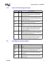
FLA[13]/
EEDI
OUT
Flash Address[13]/EEPROM Data Input.
Durin
g
Flash accesses,
this multiplexed pin acts as the Flash Address [13] output si
g
nal.
Durin
g
EEPROM accesses, it acts as serial output data to the
EEPROM Data Input si
g
nal.
FLA[12:8] OUT
Flash Address[12:8].
These pins are used as Flash address outputs
to support 128 Kb
y
te Flash addressin
g
.
FLA[7]/
CLKENB
T/S
Flash Address[7]/Clock Enable.
This is a multiplexed pin and acts
as the Flash Address[7] output si
g
nal durin
g
nominal operation. When
the PCI RST# si
g
nal is active, this pin acts as input control over the
FLA[16]/CLK25 output si
g
nal. If the FLA[7]/CLKEN pin is connected to
a pull-up resistor
(
3.3 K
Ω
)
, a 25 MHz clock si
g
nal is provided on the
FLA[16]/CLK25 output; otherwise, it is used as FLA[16] output.
FLA[6:2] OUT
Flash Address[6:2].
These pins are used as Flash address outputs
to support 128 Kb
y
te Flash addressin
g
.
FLA[1]/
AUXPWR
T/S
Flash Address[1]/Auxiliary Power.
This multiplexed pin acts as the
Flash Address[1] output si
g
nal durin
g
nominal operation. When RST is
active
(
low
)
, it acts as the power suppl
y
indicator. If the 82559ER is fed
PCI power, this pin should be connected to a pull-down resistor; if the
82559ER is fed b
y
auxiliar
y
power, this pin should be connected to a
pull-up resistor.
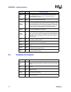
FLA[0] T/S
Flash Address [0].
This pin acts as the Flash Address[0] output
si
g
nal durin
g
nominal operation.
EECS OUT
EEPROM Chip Select.
The EEPROM Chip Select si
g
nal is used to
assert chip select to the serial EEPROM.
FLCS# OUT
Flash Chip Select.
The Flash Chip Select si
g
nal is active durin
g
Flash.
FLOE# OUT
Flash Output Enable.
This pin provides an active low output enable
control
(
read
)
to the Flash memor
y
.
FLWE# OUT
Flash Write Enable.
This pin provides an active low write enable
control to the Flash memor
y
.
Symbol Type Name and Function
Symbol Type Name and Function
TEST IN
Test.
If this input pin is hi
g
h, the 82559ER will enable the test port.
Durin
g
nominal operation this pin should be connected to a pull-down
resistor.
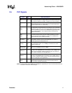
TCK IN
Testability Port Clock.
This pin is used for the Testabilit
y
Port Clock
si
g
nal.
TI IN
Testability Port Data Input.
This pin is used for the Testabilit
y
Port
Data Input si
g
nal.
TEXEC IN
Testability Port Execute Enable.
This pin is used for the Testabilit
y
Port Execute Enable si
g
nal.
TO OUT
Testability Port Data Output.
This pin is used for the Testabilit
y
Port
Data Output si
g
nal.


