


GD82559ER — Networkin
g
Silicon
54
Datasheet
7.1.13 Interru
p
t Pin Re
g
ister
The Interrupt Pin register is read only and defines which of the four PCI interrupt request pins,
INTA# through INTD#, a PCI device is connected to. The 82559ER is connected the INTA# pin.
7.1.14 Minimum Grant Re
g
ister
The Minimum Grant (Min_Gnt) register is an optional read only register for bus masters and is not
applicable to non-master devices. It defines the amount of time the bus master wants to retain PCI
bus ownership when it initiates a transaction. The default value of this register for the 82559ER is
08h. This can be converted to an actual time using the PCI specification (8* 1/PCIclk), to a value of
242ns.
7.1.15 Maximum Latenc
y
Re
g
ister
The Maximum Latency (Max_Lat) register is an optional read only register for bus masters and is
not applicable to non-master devices. This register defines how often a device needs to access the
PCI bus. The default value of this register for the 82559ER is 18h. This can be converted to an
actual time using the PCI specification (18h* 1/PCIclk), to a value of 1
µ
s.
7.1.16 Ca
p
abilit
y
ID Re
g
ister
The Capability ID is a byte register. It signifies whether the current item in the linked list is the
register defined for PCI Power Management. PCI Power Management has been assigned the value
of 01H.
7.1.17 Next Item Pointer
The Next Item Pointer is a byte register. It describes the location of the next item in the 82559ER’s
capability list. Since power management is the last item in the list, this register is set to 0b.
7.1.18 Power Mana
g
ement Ca
p
abilities Re
g
ister
The Power Management Capabilities register is a word read only register. It provides information
on the capabilities of the 82559ER related to power management. The 82559ER reports a value of
FE21h if it is connected to an auxiliary power source and 7E21h otherwise. It indicates that the
82559ER supports wake-up in the D3 state if power is supplied, either V
cc
or V
AUX
.
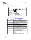
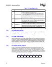
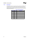
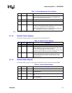
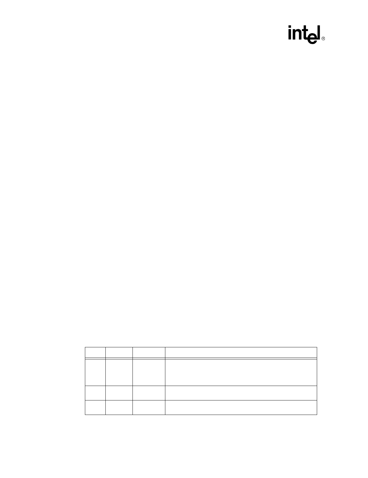
Table 8. Power Mana
g
ement Ca
p
abilit
y
Re
g
ister
Bits Default Read/Write Description
31:27 00011b
(
no V
AUX
)
11111b
(
V
AUX
)
Read Onl
y
PME Support.
This five bit field indicates the power states in which
the 82559ER ma
y
assert PME#. The 82559ER supports wake-up in
all power states if it is fed b
y
an auxiliar
y
power suppl
y
(
V
AUX
)
and
D0, D1, D2, and D3
hot
if it is fed b
y
PCI power.
26 1b Read Onl
y
D2 Support.
If this bit is set, the 82559ER supports the D2 power
state.
25 1b Read Onl
y
D1 Support.
If this bit is set, the 82559ER supports the D1 power
state.