GD82559ER — Networking Silicon
78
Datasheet
10.4.2 Timing Parameters
10.4.2.1 Measurement and Test Conditions
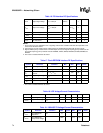
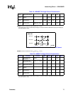
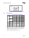
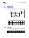
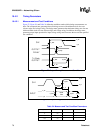
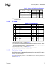
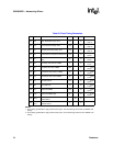
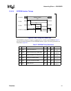
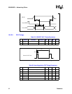
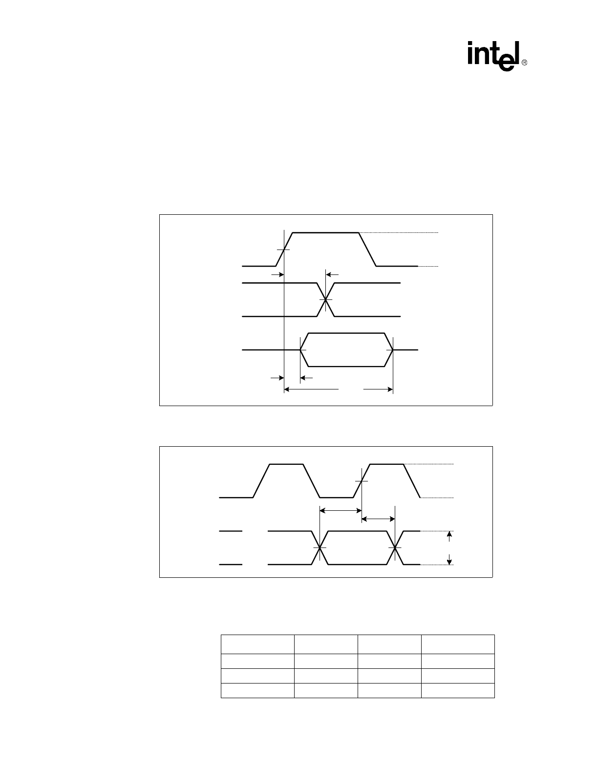
Figure 27, Figure 28, and Table 24 define the conditions under which timing measurements are
done. The component test guarantees that all timings are met with minimum clock slew rate
(slowest edge) and voltage swing. The design must guarantee that minimum timings are also met
with maximum clock slew rate (fastest edge) and voltage swing. In addition, the design must
guarantee proper input operation for input voltage swings and slew rates that exceed the specified
test conditions.
Figure 27. Output Timing Measurement Conditions
Figure 28. Input Timing Measurement Conditions
Table 24. Measure and Test Condition Parameters
Symbol PCI Level Units Notes
V
th
0.6V
CC
V
V
tl
0.2V
CC
V
V
test
0.4V
CC
V
T_off
T_on
T_val
V_ste
p
V_test V_test
V_test
V_th
V_tl
CLK
OUTPUT
DELAY
Tri-State
OUTPUT
CLK
INPUT
V_test V_test
V_test
V_th
V_tl
V_th
V_tl
T_h
T_su
in
p
uts
valid
V_max


