


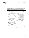
GD82559ER — Networking Silicon
80
Datasheet
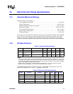
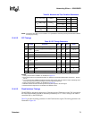
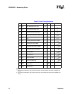
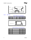
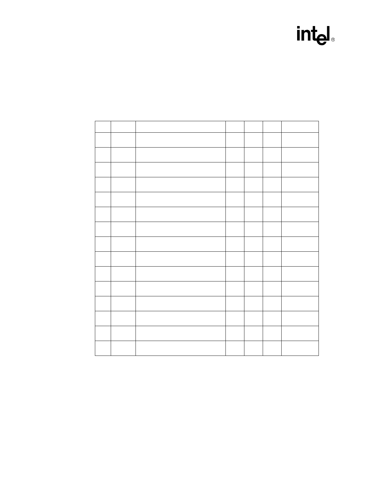
NOTES:
1. These timing specifications apply to Flash read cycles. The Flash timings referenced are 28F020-150
timings.
2. These timing specifications apply to Flash write cycles. The Flash timings referenced are 28F020-150
timings.
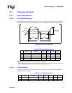
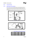
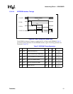
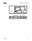
Table 26. Flash Timing Parameters
Symbol Parameter Min Max Units Notes
T35 t
flrwc
Flash Read/Write Cycle Time 150 ns
1, Flash t
AVAV
= 150 ns
T36 t
flacc
FLA to Read FLD Setup Time 150 ns
1, Flash t
AVQV
= 150 ns
T37 t
flce
FLCS# to Read FLD Setup Time 150 ns
1, Flash t
ELQV
= 150 ns
T38 t
floe
FLOE# Active to Read FLD Setup Time 120 ns
1, Flash t
GLQV
= 55 ns
T39 t
fldf
FLOE# Inactive to FLD Driven Delay
Time
50 ns
1, Flash t
GHQZ
= 35 ns
T40 t
flas
FLA Setup Time before FLWE# 5 ns
2, Flash t
AVWL
= 0 ns
T41 t
flah
FLA Hold Time after FLWE# 200 ns
2, Flash t
WLAX
= 60 ns
T42 t
flcs
FLCS# Hold Time before FLWE# 30 ns
2, Flash t
ELWL
= 20 ns
T43 t
flch
FLCS# Hold Time after FLWE# 30 ns
2, Flash t
WHEH
= 0 ns
T44 t
flds
FLD Setup Time 150 ns
2, Flash t
DVWH
= 50 ns
T45 t
fldh
FLD Hold Time 10 ns
2, Flash t
WHDX
= 10 ns
T46 t
flwp
Write Pulse Width 120 ns
2, Flash t
WLWH
= 60 ns
T47 t
flwph
Write Pulse Width High 25 ns
2, Flash t
WHWL
= 20 ns
T48 t
Mioha
IOCHRDY Hold Time after FLWE# or
FLOE# Active
25 ns
T49 t
Miohi
IOCHRDY Hold Time after FLWE# or
FLOE# Inactive
0ns