


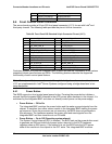
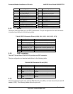
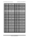
Connector/Header Locations and Pin-outs IntelP®P Server Board S3420GP TPS
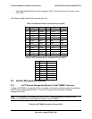
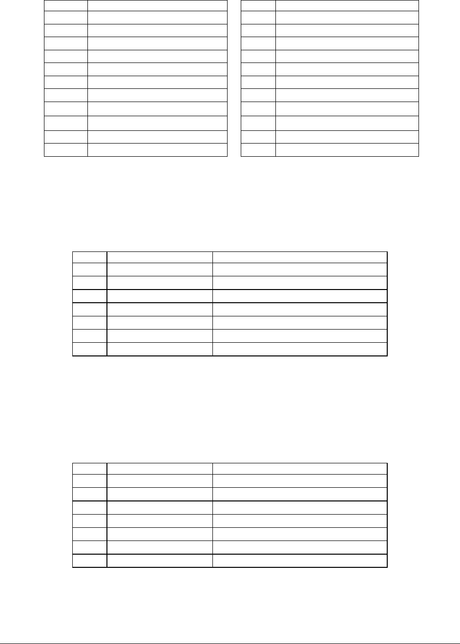
Pin Signa l Name Pin Signal Name
1 P5V_USB_PWR75 H_112 USB_PC _FB_DN
3 SB_U PCH_11_FB_DP 4 GND
5 5V_ B_DN P USB_PWR75 6 USB_PCH_10_F
7 USB_PCH_10_F B_DP 8 GND
9 P1V8_PHY_VCT_R 10 NIC1_MDIP<0>
11 NIC1_MDIN<0> 12 NIC1_MDIP<1>
13 NIC1_MDIN<1> 14 NIC2_MDIP<2>
15
NIC1_MDIN<2>
16
NIC2_MDIP<3>
17
NIC1_MDIN<3>
18 GND
19 LED_NIC1_LINK_ACT_0_R 20 P3V3_AUX
21 LED_NIC1_2 22 LED_NIC1_LINK1000_1
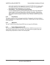
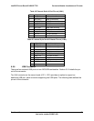
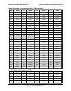
6.5.3 SATA
The sever board provides up to six SATA connectors. The pin configuration for each connector
is identical and defined in the following table.
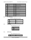
Table 43. SATA Connector Pin-out (J1H4, J1H1, J1G1, J1H3, J1G3, J1F4)
Pin Signal Name Description
1 GND Ground
2 SATA/SAS_TX_P_C Positive side of transmit differential pair
3 SATA/SAS_TX_N_C Negative side of transmit differential pair
4 GND Ground
5 SATA/SAS_RX_N_C Negative side of receive differential pair
6 SATA/SAS_RX_P_C Positive side of receive differential pair
7 GND Ground
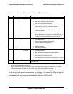
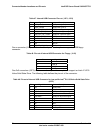
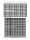
6.5.4 SAS Connectors
The Intel
®
Server Board S3420GPLX provides one SAS connector.
The pin configuration is identical and defined in the following table.
Table 44. SAS Connector Pin-out (J2H1)
Pin Signal Name Description
1 GND Ground
2 SATA/SAS_TX_P_C Positive side of transmit differential pair
3 SATA/SAS_TX_N_C Negative side of transmit differential pair
4 GND Ground
5 SATA/SAS_RX_N_C Negative side of receive differential pair
6 SATA/SAS_RX_P_C Positive side of receive differential pair
7 GND Ground
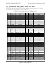
6.5.5 Serial Port Connectors
The server board provides one external DB9 Serial A port (J8A1) and one internal 9-pin serial B
header (J1B2). The following tables define the pin-outs.
Revision 1.0
Intel order number E65697-003
72