


ThunderBird Avenger
TM
PCI Audio SAA7785
Accelerator
Philips Semiconductors Preliminary Specification
1999 Nov 12 25
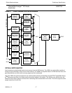
PLL/DSPCLK SUBSYSTEM INTERFACE
POWER AND GROUND PINS
CCLK CODEC Clock Input
This pin is the raw 24.576MHz clock from the AC’97 crystal. The CCLK clock is used to provide
a fixed time base for many functions within the SAA7785 device.
DSPCLK DSP Clock Input
This pin can be used as the clock input for the SAA7785 for the DSP subsystem in place of the
PLL driving the clock. DSPCLK is also used to drive the DSP subsystem for controllability dur-
ing testing.
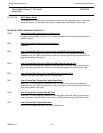
PSUB PLL Substrate
This pin supplies the bias for the guard ring on the PLL core. Connect this to a clean analog
supply ground.
PLLAPWR PLL Analog Power
Analog power supply for the PLL. Be sure the analog supply is isolated from the 3 volt digital
supply.
PLLAGND PLL Analog Ground
Analog ground for the PLL. This power supply is sensitive to noise and should be handled care-
fully.
VDDIC Core Power
3 volt power supply for the core of the chip.
VSSIC Core Ground
Ground reference for the core of the chip.
VSS Ring Ground
Ground reference for the pad interfaces of the chip.
VDD Ring Power
3 volt supply for the pad interfaces of the chip.
NWELL External N-Well Bias
Tie these pins to 5v for proper 5 volt tolerant operation. The 5v supply must be powered up
before the 3v supply. Likewise, the 3v supply must be powered down before the 5v supply.
PLEASE READ THE CAUTIONS IN Section 4.1, POWER SUPPLY OPERATING REQUIRE-
MENTS ***** MUST READ *****