


ThunderBird Avenger
TM
PCI Audio SAA7785
Accelerator
Philips Semiconductors Preliminary Specification
1999 Nov 12 36
Note: An RC indicates that this bit can be reset to 0 by writing a 1. Writing a zero leaves this bit unchanged.
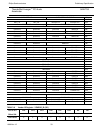
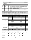
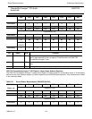
TABLE 14 Revision ID Register - REVISION (RO)
Bit Name R/W Function
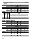
15 R_PERR RC Received Parity Error: When set to 1, this bit indicates that the SSA7785
ThunderBird Avenger™, function 0 has detected a PCI bus parity error at
least once since this bit was last reset.
14 S_SERR RC Signalled System Error: When set to 1, this bit indicates that the SSA7785
ThunderBird Avenger™, function 0 has reported a system error on the
SERR# signal at least once since this bit was last reset.
13 SM_ABORT RC Signalled Master Abort: When set to 1, this bit indicates that the SSA7785
ThunderBird Avenger™, function 0 (acting as a master) had to initiate a mas-
ter abort at least once since this bit was last reset.
12 RT_ABORT RC Received Target Abort: When set to 1, this bit indicates that the SSA7785
ThunderBird Avenger™, function 0 (acting as a master) has received a target
abort at least once since this bit was last reset.
11 ST_ABORT RC Signalled Target Abort: When set to 1, this bit indicates that the SSA7785
ThunderBird Avenger™, function 0 has signalled a target abort at least once
since this bit was last reset.
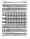
10:9 DEVSEL_TM
G
RO DEVSEL Timing: This field indicates the timing of the DEVSEL output (when
a PCI master is accessing a SSA7785 ThunderBird Avenger™, function 0
resource). It always returns 01 (Bin).
00 = Fast
01 = Medium (Default Timing)
10 = Slow
8 S_PERR RC Signalled Parity Error: When set to 1, this bit indicates that the SSA7785
ThunderBird Avenger™, function 0 was a bus master for a cycle in which
PERR# was activated. This bit cannot be set if the PERR_RESP bit in the
command register is not enabled.
7 F_BK2BK RO Always returns 1 to indicate support of fast back to back cycles when the
SSA7785 ThunderBird Avenger™, function 0 is the target.
6 UDF RO User Definable Features. Always returns 0.
5 MHz66 RO 66 MHzMHz Capable. Always returns 0.
4:0 R RO Reserved. These bits always return zero.
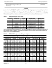
PCI CFG 0D7D6D5D4D3D2D1D0
Offset 08h
REVISION_ID[7:0]
POR Value
00011001