


ThunderBird Avenger
TM
PCI Audio SAA7785
Accelerator
Philips Semiconductors Preliminary Specification
1999 Nov 12 27
SAA7785 ThunderBird Avenger™ Functional Block Descriptions
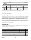
Register Table Document Description and Example
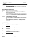
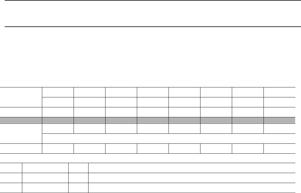
The next table gives an example of how registers are documented in this specification.
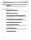
TABLE 4 Example Register - REGEX (RW/RO)
In the above table example, the EXAMPLE REGISTER text would be a descriptive title for the register that we wish to
detail. Following the register description would be a register mnemonic used in register summary tables and the like. In
this example the mnemonic is REGEX. Following the mnemonic is the read/write access allowed into this register. If the
entire register is readable and writable, then the RW key is assigned. If some bits are read/write while others are read
only, then the key will indicate this fact. In the example, this register has both read/write and read only bits. The register
memory map location is marked in the table cell marked SPACE. SPACE could be substituted with PCI CFG n (for PCI
configuration register space for function n), IOBASE (for an I/O space register with an IOBASE specified in a configura-
tion register), DSP DATA (for DSP data memory mapped registers), MEM MSTR (indicating a PCI master in memory
space), and DSP CODE (indicating a DSP code memory mapped register. Just below the SPACE marker is the offset
from the base address specified in the SPACE field. The rest of the table should be obvious.
SAA7785 ThunderBird Avenger™ PCI Interface
Overview
The SSA7785 ThunderBird Avenger™ chip PCI interface is designed to interface the external PCI bus interface to all of
the selected devices in the SSA7785 ThunderBird Avenger™ chip. The PCI interface composed of master and slave
state machines, an address/data/byte enable datapath, a bus arbiter for the two on chip masters, control logic for the
master and slave internal busses, and standard PCI configuration register headers. The Interrupt Serializer will be dis-
cussed in a later chapter. This section of the specification will describe the PCI interface in more detail along with
design considerations for both the slave, master, and datapath. The configuration header will be discussed in the
SSA7785 ThunderBird Avenger™ PCI Configuration Registers section of this specification.
The discussion will begin with the PCI master and target systems. The PCI bus master has the capability to burst dou-
ble words to/from the two internal bus masters, the Distributed DMA and the Virtual Registers. The full address range is
supported for these master devices. Since there are two masters, an arbiter is required to determine priority between
the two devices. Details on the arbiter can be found in the PCI master section.
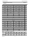
SPACE D15 D14 D13 D12 D11 D10 D9 D8
Offset nnh RRRRRRRR
POR Value 00000000
D7 D6 D5 D4 D3 D2 D1 D0
EXDATA[7:0]
POR Value 00000000
Bit Name R/W Function
15:8 R RO Reserved. These bits always return zeros.
7:0 EXDATA RW Example data. The example data for all to see.