


ThunderBird Avenger
TM
PCI Audio SAA7785
Accelerator
Philips Semiconductors Preliminary Specification
1999 Nov 12 49
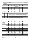
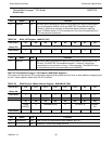
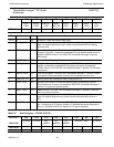
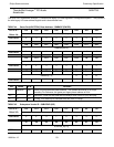
TABLE 37 Status Register - STATUS (RO/RW)
D7 D6 D5 D4 D3 D2 D1 D0
STEP-
PING
PERR_
RESP
SNOOP_
ENB
MEM_
INV_EN
SPEC_
CNTL
MAST_
CNTL
MEM_
CNTL
IO_
CNTL
POR Value
00000000
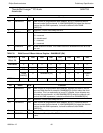
Bit Name R/W Function
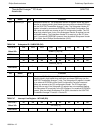
15:10 R RO Reserved. These bits always return zero.
9 FBACK_ENB RO Fast Back-to-Back Enable: the SSA7785 ThunderBird Avenger™, function 1
does not support fast back to back master cycles therefore this bit always
returns a zero.
8 SERR_RESP RW System Error Response: When set to 1, the SSA7785 ThunderBird
Avenger™, function 1 responds to detected PCI bus address parity errors by
asserting SERR#. When 0, the SSA7785 ThunderBird Avenger™ ignores
these errors.
7 STEPPING RO Address / Data Stepping: Always returns 0.
6 PERR_RESP RW Parity Error Response: When set to 1, the SSA7785 ThunderBird Avenger™,
function 1 responds to detected PCI bus data parity errors by asserting
PERR#. When 0, the SSA7785 ThunderBird Avenger™ ignores PCI bus data
parity errors.
5 SNOOP_ENB RO VGA Snoop Enable. The SSA7785 ThunderBird Avenger™, function 1 does
not support VGA snoop enable, therefor this bit always returns a zero.
4 MEM_INV_EN RO Memory Write and Invalidate Enable: Always returns 0.
3 SPEC_CNTL RO Special Cycle Control: Controls the devices ability to respond to Special
Cycle Operations. A value of 0 causes the SSA7785 ThunderBird Avenger™,
function 1 to ignore all Special Cycles.
2 MAST_CNTL RO Master Control: The SSA7785 ThunderBird Avenger™, function 1 does not
have any master functions.
1 MEM_CNTL RO Memory Response Control: The SSA7785 ThunderBird Avenger™, function 1
does not support target memory cycles therefore this bit always returns a
zero.
0 IO_CNTL RW I/O Response Control: Controls the SSA7785 ThunderBird Avenger™, func-
tion 1’s response to I/O space. A value of 0 disables the device response. A
value of 1 allows the device to respond to I/O space accesses.
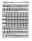
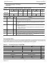
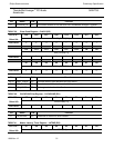
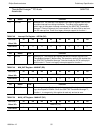
PCI CFG 1 D15 D14 D13 D12 D11 D10 D9 D8
Offset 06h
R_PERR S_SERR SM_
ABORT
RT_
ABORT
ST_
ABORT
DEVSEL_TMG S_PERR
POR Value
00000010