


ThunderBird Avenger
TM
PCI Audio SAA7785
Accelerator
Philips Semiconductors Preliminary Specification
1999 Nov 12 45
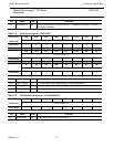
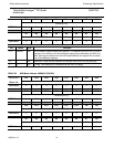
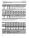
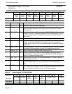
TABLE 29 MAX_LAT Register - MAXLAT (RO)
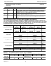
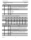
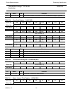
SSA7785 ThunderBird Avenger™ CFG Space 0 DMA Base Registers
This section will describe the PCI configuration registers that provide functions such as base address remapping and
the like. These registers reside within the PCI interface.
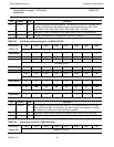
TABLE 30 DMA Channel A Base Address Register - DMAABASE (RW)
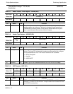
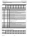
Bit Name R/W Function
7:0 MINGNT RO Minimum grant specifies how long of a burst period the device needs assum-
ing a clock speed of 33MHz. Since the SSA7785 ThunderBird Avenger™,
function 0, will burst a maximum of 64 double words, therefore requiring
about 75 33MHz clocks or 2.25 microseconds. The time units specified are in
0.25 microsecond increments.
PCI CFG 0D7D6D5D4D3D2D1D0
Offset 3Fh
MAXLAT[7:0]
POR Value
00101000
Bit Name R/W Function
7:0 MAXLAT RO Maximum latency specifies how often a device needs to gain access to the
PCI bus. The SSA7785 ThunderBird Avenger™, function 0, should only
request the bus a a maximum of every 10 microseconds. The MAXLAT value
is computed using the same parameters as the MINGNT.
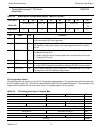
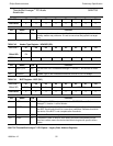
PCI CFG 0 D15 D14 D13 D12 D11 D10 D9 D8
Offset 40h
DMAABASE[15:8]
POR Value
00000000
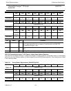
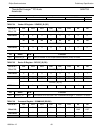
D7 D6 D5 D4 D3 D2 D1 D0
DMAA
BASE[7]
R DMAABASE[5:4] R XFRSIZ[1:0] DDMAA
EN
POR Value
00000100
Bit Name R/W Function
15:7 DMAABASE RW DMA channel A programmable base address, bits 15:7.
6 R RO Reserved. This bit must always be zero.