APPLICATION
2.3 Timers
2-28
4513/4514 Group User’s Manual
(3) Timer control register W1
The timer 1 count start synchronous circuit control bit is assigned to bit 0, the timer 1 control bit is
assigned to bit 1, the prescaler dividing ratio selection bit is assigned to bit 2, and the prescaler
control bit is assigned to bit 3.
Set the contents of this register through register A with the TW1A instruction. The TAW1 instruction
can be used to transfer the contents of register W1 to register A.
Table 2.3.3 shows the timer control register W1.
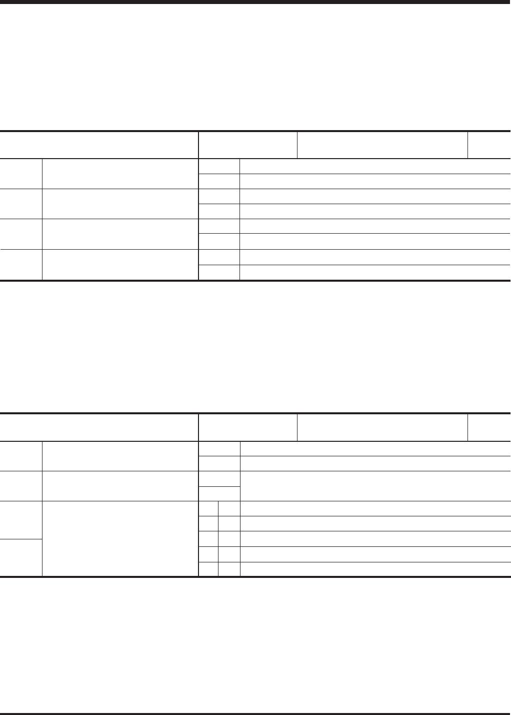
Table 2.3.3 Timer control register W1
Timer control register W1 at reset : 00002 at RAM back-up : 00002
R/W
Stop (state initialized)
Operating
Instruction clock divided by 4
Instruction clock divided by 16
Stop (state retained)
Operating
Count start synchronous circuit not selected
Count start synchronous circuit selected
Prescaler control bit
Prescaler dividing ratio selection
bit
Timer 1 control bit
Timer 1 count synchronous circuit
control bit
W13
W12
W11
W10
0
1
0
1
0
1
0
1
Note: “R” represents read enabled, and “W” represents write enabled.
(4) Timer control register W2
The timer 2 count source selection bits are assigned to bits 0 and 1, and the timer 2 control bit is
assigned to bit 3.
Set the contents of this register through register A with the TW2A instruction. The TAW2 instruction
can be used to transfer the contents of register W2 to register A.
Table 2.3.4 shows the timer control register W2.
Table 2.3.4 Timer control register W2
Timer control register W2 at reset : 00002 at RAM back-up : state retained
R/W
Stop (state retained)
Operating
This bit has no function, but read/write is enabled.
Count source
Timer 1 underflow signal
Prescaler output
CNTR0 input
16-bit timer (WDT) underflow signal
Timer 2 control bit
Not used
Timer 2 count source selection
bits
W23
W22
W21
W20
0
1
0
1
Note: “R” represents read enabled, and “W” represents write enabled.
W21
0
0
1
1
W20
0
1
0
1


