


1-12
HARDWARE
4513/4514 Group User’s Manual
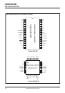
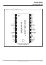
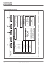
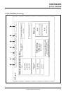
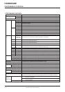
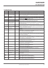
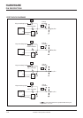
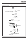
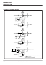
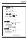
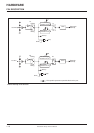
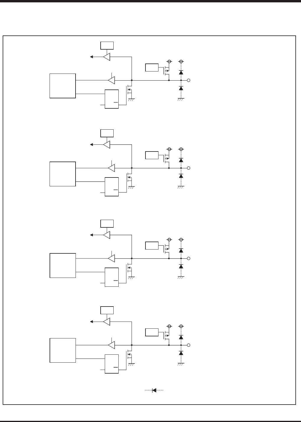
PORT BLOCK DIAGRAMS
PIN DESCRIPTION
D
T
Q
Ai
P00,P01
K0
0
PU0
0
D
T
Ai
P02,P03
K0
1
PU0
1
D
T
Ai
P10,P11
K0
2
PU0
2
D
T
Ai
P12,P13
K0
3
PU0
3
Key-on wakeup input
Pull-up
transistor
OP0A instruction
IAP0 instruction
Key-on wakeup input
Pull-up
transistor
OP0A instruction
IAP0 instruction
Key-on wakeup input
Pull-up
transistor
OP1A instruction
IAP1 instruction
Key-on wakeup input
Pull-up
transistor
Register A
OP1A instruction
IAP1 instruction
This symbol represents a parasitic diode on the port.
i represents 0, 1, 2, or 3.
•
•
Register A
Register A
Register A
Q
Q
Q