


APPLICATION
2.5 A-D converter
2-49
4513/4514 Group User’s Manual
2.5 A-D converter
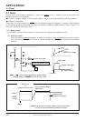
The 4513/4514 Group has an A-D converter with the 10-bit successive comparison method: 4 channels for
the 4513 Group, 8 channels for the 4514 Group.
This A-D converter can also be used as a comparator to compare analog voltages input from the analog
input pin with preset values.
This section describes the related registers, application examples using the A-D converter and notes.
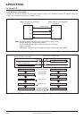
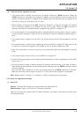
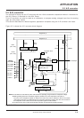
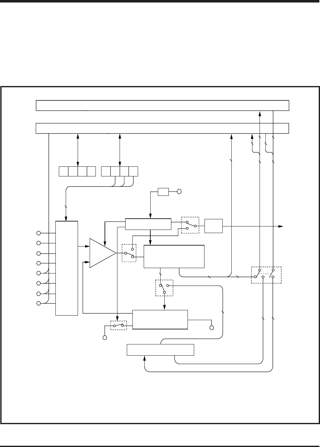
Figure 2.5.1 shows the A-D converter block diagram.
Fig. 2.5.1 A-D converter structure
Register A (4)
V
SS
V
DD
IAP4
(P4
0
—
P4
3
)
TABAD
1/6
Q2
3
Register B (4)
Q1
1
Q1
0
Q1
2
TADAB
Q2
2
Q2
1
Q2
0
0
1
4
4
4
4
8 8
8
01
1
8
10
Q2
3
Q2
3
DAC
operation
signal
0
1
Q2
3
8
8
2
TALA
Q2
3
Q1
3
TAQ1
TQ1A
TAQ2
TQ2A
ADF
(1)
A
IN0
/CMP0-
A
IN1
/CMP0+
A
IN2
/CMP1-
A
IN3
/CMP1+
P4
0
/A
IN4
P4
1
/A
IN5
P4
2
/A
IN6
P4
3
/A
IN7
3
10
10
Comparator
8-channel multi-plexed analog switch
Instruction clock
A-D control circuit
Successive comparison
register (AD) (10)
A-D interrupt
DA converter
(Note 1)
Comparator register (8)
(Note 2)
Notes 1: This switch is turned ON only when A-D converter is operating and generates the comparison voltage.
2: Writing/reading data to the comparator register is possible only in the comparator mode (Q2
3
=1).
The value of the comparator register is retained even when the mode is switched to the A-D conversion
mode (Q2
3
=0) because it is separated from the successive comparison register (AD). Also, the resolution in
the comparator mode is 8 bits because the comparator register consists of 8 bits.
3: The 4513 Group does not have ports P4
0
/A
IN4
–P4
3
/A
IN7
and the IAP4 and OP4A instructions.
(Note 3)
OP4A
(P4
0
—
P4
3
)