APPLICATION
2-59
4513/4514 Group User’s Manual
2.9 RAM back-up
2.9 RAM back-up
2.9.1 RAM back-up mode
The system enters RAM back-up mode when the POF instruction is executed after the EPOF instruction
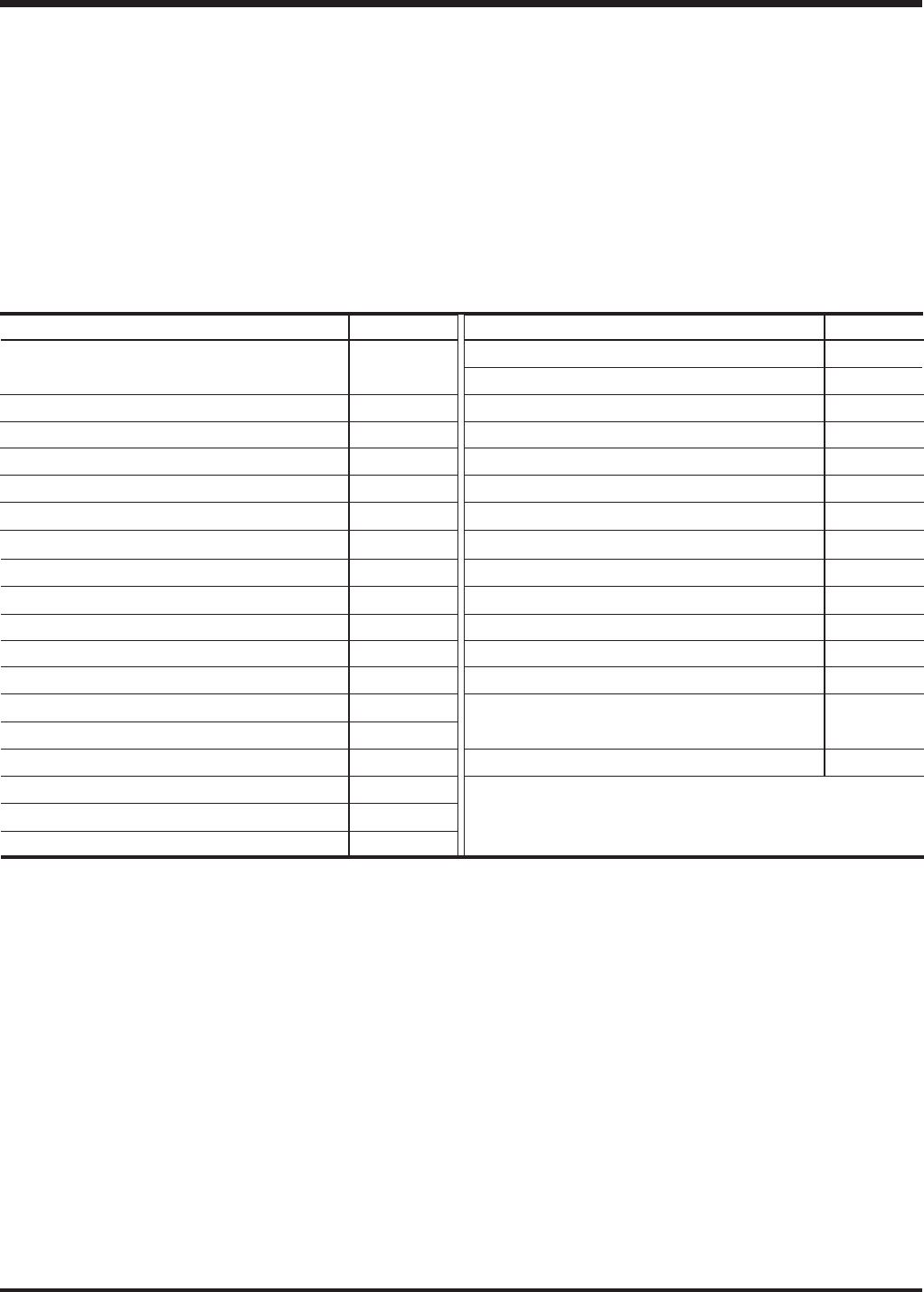
is executed. Table 2.9.1 shows the function and state retained at RAM back-up mode. Also, Table 2.9.2
shows the return source from this state.
(1) RAM back-up mode
As oscillation stops with RAM, the state of reset circuit retained, current dissipation can be reduced
without losing the contents of RAM.
Function
Program counter (PC), registers A, B,
carry flag (CY), stack pointer (SP) (Note 2)
Contents of RAM
Port level
Timer control register W1
Timer control registers W2 to W4. W6
Clock control register MR
Interrupt control registers V1, V2
Interrupt control registers I1, I2
Timer 1 function
Timer 2 function
Timer 3 function
Timer 4 function
A-D function
A-D control registers Q1, Q2
Voltage comparator function
Voltage comparator control register Q3
Serial I/O function
Serial I/O mode register J1
RAM back-up
✕
O
O
✕
O
✕
✕
O
✕
(Note 3)
(Note 3)
(Note 3)
✕
O
O (Note 5)
O
✕
O
Table 2.9.1 Functions and states retained at RAM back-up mode
Function
Pull-up control register PU0
Key-on wakeup control register K0
Direction register FR0
External 0 interrupt request flag (EXF0)
External 1 interrupt request flag (EXF1)
Timer 1 interrupt request flag (T1F)
Timer 2 interrupt request flag (T2F)
Timer 3 interrupt request flag (T3F)
Timer 4 interrupt request flag (T4F)
Watchdog timer flags (WDF1, WDF2)
Watchdog timer enable flag (WEF)
16-bit timer (WDT)
A-D conversion completion flag (ADF)
Serial I/O transmit/receive completion flag
(SIOF)
Interrupt enable flag (INTE)
RAM back-up
O
O
O
✕
✕
✕
(Note 3)
(Note 3)
(Note 3)
✕ (Note 4)
✕ (Note 4)
✕ (Note 4)
✕
✕
✕
Notes 1: “O” represents that the function can be retained, and “✕” represents that the function is initialized.
Registers and flags other than the above are undefined at RAM back-up, and set an initial value
after returning.
2: The stack pointer (SP) points the level of the stack register and is initialized to “7” at RAM back-
up.
3: The state of the timer is undefined.
4: Initialize the watchdog timer with the WRST instruction, and then execute the POF instruction.
5: The state is retained when the voltage comparator function is selected with the voltage comparator
control register Q3.


