3-22
APPENDIX
3.3 List of precautions
4513/4514 Group User’s Manual
➉ A-D converter-1
When the operating mode of the A-D converter is changed from
the comparator mode to the A-D conversion mode with the bit 3
of register Q2 in a program, be careful about the following notes.
• Clear the bit 2 of register V2 to “0” to change the operating mode
of the A-D converter from the comparator mode to the A-D con-
version mode with the bit 3 of register Q2 (refer to Figure 46➄).
• The A-D conversion completion flag (ADF) may be set when the
operating mode of the A-D converter is changed from the com-
parator mode to the A-D conversion mode. Accordingly, set a
value to register Q2, and execute the SNZAD instruction to clear
the ADF flag.
Do not change the operating mode (both A-D conversion mode
and comparator mode) of A-D converter with the bit 3 of register
Q2 during operating the A-D converter.
.
.
.
LA 8 ; (✕0✕✕2)
TV2A ; The SNZAD instruction is valid ........➄
LA 0 ; (0✕✕✕2)
TQ2A ; Change of the operating mode of the A-D
converter from the comparator mode to the
A-D conversion mode
SNZAD
NOP
.
.
.
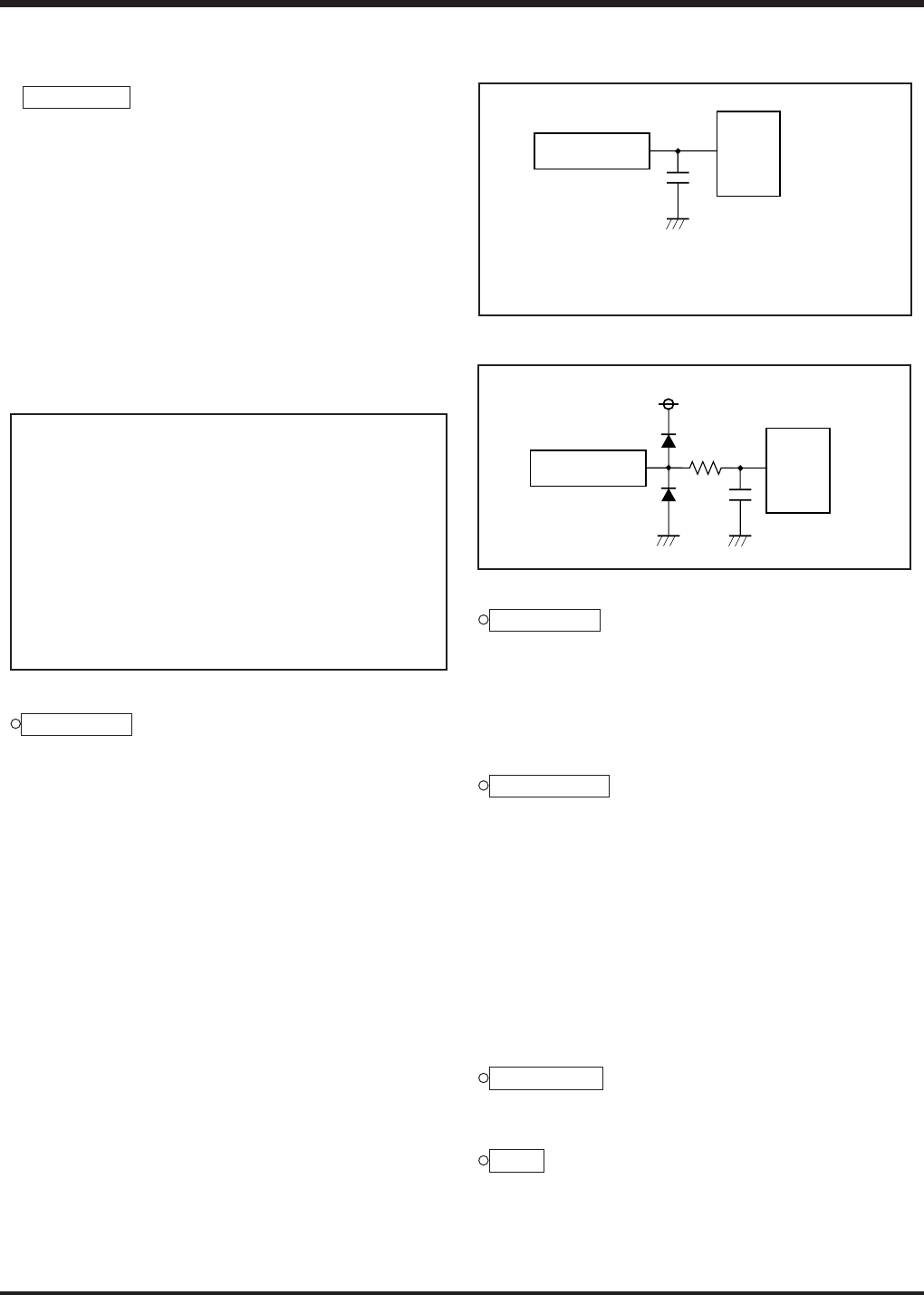
Fig. 47 Analog input external circuit example-1
Fig. 48 Analog input external circuit example-2
POF instruction
Execute the POF instruction immediately after executing the
EPOF instruction to enter the RAM back-up.
Note that system cannot enter the RAM back-up state when ex-
ecuting only the POF instruction.
Be sure to disable interrupts by executing the DI instruction be-
fore executing the EPOF instruction.
Analog input pins
Note the following when using the analog input pins also for I/O
port P4 functions:
• Even when P40/AIN4–P43/AIN7 are set to pins for analog input,
they continue to function as P40–P43 I/O. Accordingly, when any
of them are used as I/O port P4 and others are used as analog
input pins, make sure to set the outputs of pins that are set for
analog input to “1.” Also, the port input function of the pin func-
tions as an analog input is undefined.
• TALA instruction
When the TALA instruction is executed, the low-order 2 bits of
register AD is transferred to the high-order 2 bits of register A, si-
multaneously, the low-order 2 bits of register A is “0.”
Program counter
Make sure that the PCH does not specify after the last page of
the built-in ROM.
Port P3
In the 4513 Group, when the IAP3 instruction is executed, note
that the high-order 2 bits of register A is undefined.
A-D converter-2
Each analog input pin is equipped with a capacitor which is used
to compare the analog voltage. Accordingly, when the analog
voltage is input from the circuit with high-impedance and, charge/
discharge noise is generated and the sufficient A-D accuracy
may not be obtained. Therefore, reduce the impedance or, con-
nect a capacitor (0.01 µF to 1 µF) to analog input pins (Figure
47).
When the overvoltage applied to the A-D conversion circuit may
occur, connect an external circuit in order to keep the voltage
within the rated range as shown the Figure 48. In addition, test
the application products sufficiently.
✕: this bit is not related to the change of the
operating mode of the A-D conversion.
Fig. 46 A-D converter operating mode program example
11
Sensor
AIN
Apply the voltage withiin the specifications
to an analog input pin.
Sensor
AIN
About 1kΩ
12
13
14
15


