


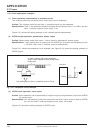
APPLICATION
2.3 Timers
2-33
4513/4514 Group User’s Manual
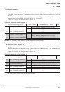
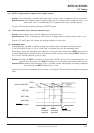
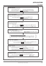
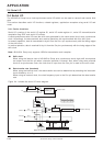
Fig. 2.3.4 CNTR0 output setting example
g0 h
0
b3 b0
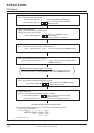
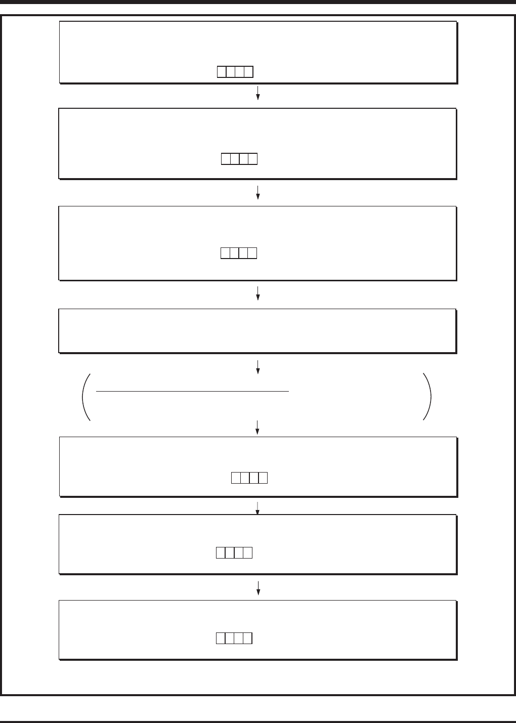
➀ Disable Interrupts
Timer 1 interrupt is temporarily disabled.
Interrupt enable flag INTE
Interrupt control register V1
“0”
✕✕✕
All interrupts disabled (DI instruction)
Timer 1 interrupt occurrence disabled
(TV1A instruction)
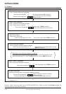
b3 b0
00
➁ Stop Timer Operation
Timer 1 and prescaler are temporarily stopped.
Dividing ratio of prescaler is selected.
Timer control register W1
✕
Timer 1 stop (TW1A instruction)
Prescaler stop
Prescaler divided by 4 selected
0
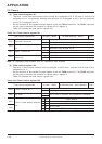
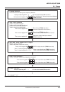
➂ Set Timer Value, Select CNTR0 Output
CNTR0 output is selected.
Timer 1 count time is set.
Timer control register W6
Timer 1 reload register R1
“29
16”
Timer count value 41 set (T1AB instruction)
b3 b0
1
✕
0
✕
CNTR0 output selected (TW6A instruction)
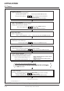
➃ Clear Interrupt Request
Timer 1 interrupt activated condition is cleared.
Timer 1 interrupt request flag T1F
“0”
Timer 1 interrupt activated condition cleared
(SNZT1 instruction)
Note when the interrupt request is cleared
When ➃ is executed, considering the skip of the next instruction according to the
interrupt request flag T1F, insert the NOP instruction after the SNZT1 instruction.
➄ Start Timer 1 Operation
Timer 1 and prescaler temporarily stopped are restarted.
Timer 1 operation start (TW1A instruction)
Prescaler operation start
b3 b0
10
Timer control register W1
✕
1
b3 b0
1
➅ Enable Interrupts
The timer 1 interrupt which is temporarily disabled is enabled.
Interrupt control register V1
Interrupt enable flag INTE
“1”
Timer 1 interrupt occurrence enabled
(TV1A instruction)
All interrupts enabled (EI instruction)
✕✕✕
b3 b0
0
➆ Stop CNTR0 Output
D6/CNTR0 pin is set to CNTR0 input pin, and it is set to the high-impedance state.
Timer control register W6
Output latch of port D
6 is set to “1.”
CNTR0 input pin set (TW6A instruction)
(SD instruction)
✕✕
0
“✕”: it can be “0” or “1.”