4513/4514 Group User’s Manual
HARDWARE
1-45
FUNCTION BLOCK OPERATIONS
(10) Operation at comparator mode
The A-D converter is set to comparator mode by setting bit 3 of the
register Q2 to “1.”
Below, the operation at comparator mode is described.
(11) Comparator register
In comparator mode, the built-in DA comparator is connected to the
comparator register as a register for setting comparison voltages.
The contents of register B is stored in the high-order 4 bits of the
comparator register and the contents of register A is stored in the
low-order 4 bits of the comparator register with the TADAB instruc-
tion.
When changing from A-D conversion mode to comparator mode,
the result of A-D conversion (register AD) is undefined.
However, because the comparator register is separated from regis-
ter AD, the value is retained even when changing from comparator
mode to A-D conversion mode. Note that the comparator register
can be written and read at only comparator mode.
If the value in the comparator register is n, the logic value of com-
parison voltage Vref generated by the built-in DA converter can be
determined from the following formula:
(12) Comparison result store flag (ADF)
In comparator mode, the ADF flag, which shows completion of A-D
conversion, stores the results of comparing the analog input volt-
age with the comparison voltage. When the analog input voltage is
lower than the comparison voltage, the ADF flag is set to “1.” The
state of ADF flag can be examined with the skip instruction
(SNZAD). Use the interrupt control register V2 to select the inter-
rupt or the skip instruction.
The ADF flag is cleared to “0” when the interrupt occurs or when
the next instruction is skipped with the skip instruction.
(13) Comparator operation start instruction
(ADST instruction)
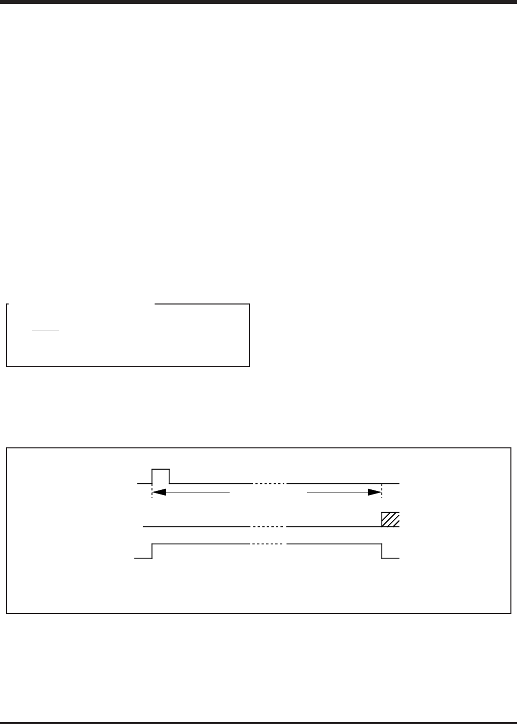
In comparator mode, executing ADST starts the comparator oper-
ating.
The comparator stops 8 machine cycles after it has started (6
µ
s at
f(XIN) = 4.0 MHz in high-speed mode). When the analog input volt-
age is lower than the comparison voltage, the ADF flag is set to “1.”
(14) Notes for the use of A-D conversion 1
Note the following when using the analog input pins also for I/O
port P4 functions:
• Even when P40/AIN4–P43/AIN7 are set to pins for analog input,
they continue to function as P40–P43 I/O. Accordingly, when any
of them are used as I/O port P4 and others are used as analog
input pins, make sure to set the outputs of pins that are set for
analog input to “1.” Also, the port input function of the pin func-
tions as an analog input is undefined.
• TALA instruction
When the TALA instruction is executed, the low-order 2 bits of
register AD is transferred to the high-order 2 bits of register A, si-
multaneously, the low-order 2 bits of register A is “0.”
Logic value of comparison voltage Vref
Vref = ✕ n
n: The value of register AD (n = 0 to 255)
Fig. 29 Comparator operation timing chart
VDD
256
ADST instruction
Comparison result
store flag(ADF)
8 machine cycles
DAC operation signal
Comparator operation completed.
(
Th
e
v
a
l
ue
o
f ADF i
s
de
t
e
rmin
ed)
→


