


APPENDIX
3.1 Electrical characteristics
3-6
4513/4514 Group User’s Manual
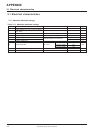
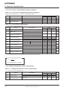
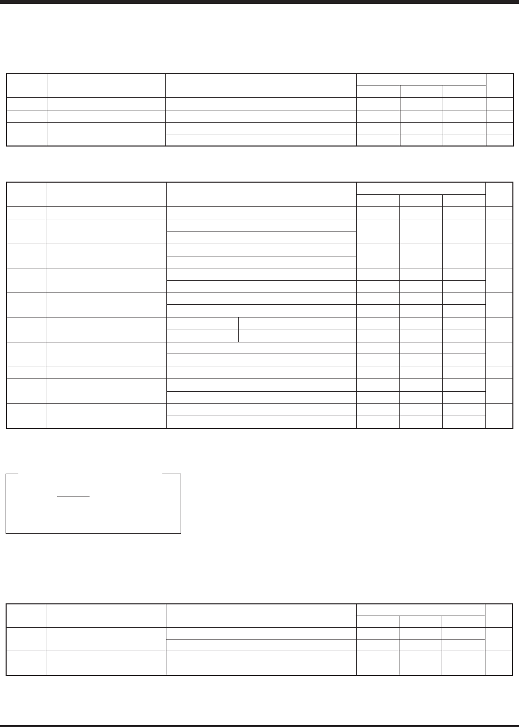
3.1.4 A-D converter recommended operating conditions
Table 3.1.5 A-D converter recommended operating conditions
(Comparator mode included, Ta = –20 °C to 85 °C, unless otherwise noted)
Symbol
VDD
VIA
f(XIN)
Parameter
Supply voltage
Analog input voltage
Oscillation frequency
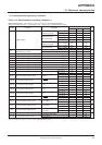
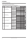
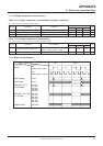
Table 3.1.6 A-D converter characteristics
(Ta = –20 °C to 85 °C, unless otherwise noted)
Conditions Unit
V
V
MHz
MHz
Middle-speed mode, VDD ≥ 2.7 V
High-speed mode, VDD ≥ 2.7 V
Min.
2.7
0
0.8
0.4
Typ. Max.
5.5
VDD
Limits
Symbol
–
–
–
V0T
VFST
IADD
TCONV
–
–
–
Parameter
Resolution
Linearity error
Differential non-linearity error
Zero transition voltage
Full-scale transition voltage
A–D operating current
A-D conversion time
Comparator resolution
Comparator error (Note)
Comparator comparison time
Test conditions
Unit
bits
LSB
LSB
mV
mV
mA
µ
s
bits
mV
µ
s
Ta = 25 °C, VDD = 2.7 V to 5.5 V
Ta = –25 °C to 85 ° C, VDD = 3.0 V to 5.5 V
Ta = 25 °C, VDD = 2.7 V to 5.5 V
Ta = –25 °C to 85 ° C, VDD = 3.0 V to 5.5 V
VDD = 5.12 V
VDD = 3.072 V
VDD = 5.12 V
VDD = 3.072 V
VDD = 5.0 V
VDD = 3.0 V
f(XIN) = 4.0 MHz, Middle-speed mode
f(XIN) = 4.0 MHz, High-speed mode
Comparator mode
VDD = 5.12 V
VDD = 3.072 V
f(XIN) = 4.0 MHz, Middle-speed mode
f(XIN) = 4.0 MHz, High-speed mode
Min.
0
0
5105
3060
Typ.
5
3
5115
3069
0.7
0.2
Max.
10
±2
±0.9
20
15
5125
3075
2.0
0.4
93.0
46.5
8
±20
±15
12
6
Limits
f(XIN) = 0.4 MHz to 4.0 MHz
f(XIN) = 0.4 MHz to 2.0 MHz
Note: As for the error from the ideal value in the comparator mode, when the contents of the comparator register is n, the logic value of the comparison volt-
age V
ref which is generated by the built-in DA converter can be obtained by the following formula.
Logic value of comparison voltage Vref
Vref = ✕ n
n = Value of register AD (n = 0 to 255)
VDD
256
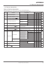
3.1.5 Voltage drop detection circuit characteristics
Table 3.1.7 Voltage drop detection circuit characteristics
(Ta = –20 °C to 85 °C, unless otherwise noted)
Test conditions
Ta = 25 °C
VDD = 5.0 V
Parameter
Detection voltage
Operation current of voltage
drop detection circuit
Symbol
VRST
IRST
Limits
Unit
V
µ
A
Min.
2.7
3.3
Ty p.
3.5
50
Max.
4.1
3.7
100