


1-42
HARDWARE
4513/4514 Group User’s Manual
FUNCTION BLOCK OPERATIONS
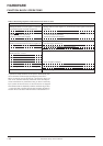
Q13
Q12
Q11
Q10
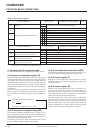
A-D control register Q1
Not used
Analog input pin selection bits (Note 2)
at reset : 00002 at RAM back-up : state retained
0
1
Q12
0
0
0
0
1
1
1
1
Q11
0
0
1
1
0
0
1
1
This bit has no function, but read/write is enabled.
Selected pins
AIN0
AIN1
AIN2
AIN3
AIN4 (Not available for the 4513 Group)
AIN5 (Not available for the 4513 Group)
AIN6 (Not available for the 4513 Group)
AIN7 (Not available for the 4513 Group)
at reset : 00002
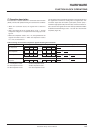
Q23
Q22
Q21
Q20
A-D control register Q2
A-D conversion mode
Comparator mode
P43, P42 (read/write enabled for the 4513 Group)
AIN7, AIN6/P43, P42(read/write enabled for the 4513 Group)
P41 (read/write enabled for the 4513 Group)
AIN5/P41 (read/write enabled for the 4513 Group)
P40 (read/write enabled for the 4513 Group)
AIN4/P40 (read/write enabled for the 4513 Group)
A-D operation mode selection bit
P43/AIN7 and P42/AIN6 pin function selec-
tion bit (Not used for the 4513 Group)
P41/AIN5 pin function selection bit
(Not used for the 4513 Group)
P40/AIN4 pin function selection bit
(Not used for the 4513 Group)
at RAM back-up : state retained
0
1
0
1
0
1
0
1
Notes 1: “R” represents read enabled, and “W” represents write enabled.
2: Select A
IN4–AIN7 with register Q1 after setting register Q2.
Q10
0
1
0
1
0
1
0
1
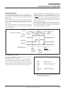
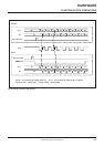
(1) Operating at A-D conversion mode
The A-D conversion mode is set by setting the bit 3 of register Q2 to “0.”
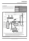
(2) Successive comparison register AD
Register AD stores the A-D conversion result of an analog input in
10-bit digital data format. The contents of the high-order 8 bits of
this register can be stored in register B and register A with the
TABAD instruction. The contents of the low-order 2 bits of this reg-
ister can be stored into the high-order 2 bits of register A with the
TALA instruction. However, do not execute this instruction during A-
D conversion.
When the contents of register AD is n, the logic value of the com-
parison voltage Vref generated from the built-in DA converter can
be obtained with the reference voltage VDD by the following for-
mula:
Logic value of comparison voltage Vref
Vref = ✕ n
n: The value of register AD (n = 0 to 1023)
VDD
1024
(4) A-D conversion start instruction (ADST)
A-D conversion starts when the ADST instruction is executed. The
conversion result is automatically stored in the register AD.
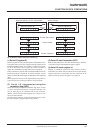
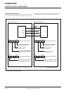
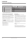
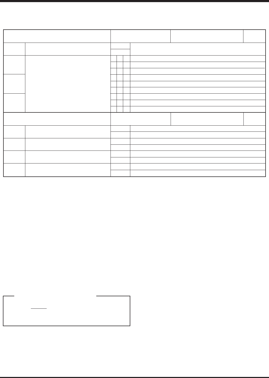
(5) A-D control register Q1
Register Q1 is used to select one of analog input pins. The 4513
Group does not have AIN4–AIN7. Accordingly, do not select these
pins with register Q1.
(6) A-D control register Q2
Register Q2 is used to select the pin function of P40/AIN4, P41/
AIN5, P42/AIN6, and P43/AIN7. The A-D conversion mode is se-
lected when the bit 3 of register Q2 is “0,” and the comparator
mode is selected when the bit 3 of register Q2 is “1.” After set this
register, select the analog input with register Q1.
Even when register Q2 is used to set the pins for analog input,
P40/AIN4–P43/AIN7 continue to function as P40–P43 I/O. Accord-
ingly, when any of them are used as I/O port P4 and others are
used as analog input pins, make sure to set the outputs of pins that
are set for analog input to “1.” Also, for the port input, the port input
function of the pin functions as analog input is undefined.
R/W
R/W
Table 15 A-D control registers
(3) A-D conversion completion flag (ADF)
A-D conversion completion flag (ADF) is set to “1” when A-D con-
version completes. The state of ADF flag can be examined with the
skip instruction (SNZAD). Use the interrupt control register V2 to
select the interrupt or the skip instruction.
The ADF flag is cleared to “0” when the interrupt occurs or when
the next instruction is skipped with the skip instruction.