APPLICATION
2.4 Serial I/O
2-42
4513/4514 Group User’s Manual
2.4.3 Operation description
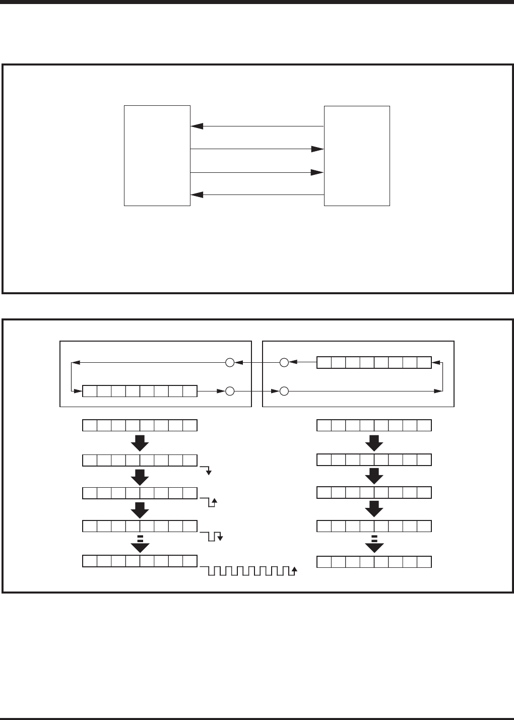
Figure 2.4.2 shows the serial I/O connection example, Figure 2.4.3 shows the serial I/O register state, and
Figure 2.4.4 shows the serial I/O transfer timing.
Fig. 2.4.2 Serial I/O connection example
Fig. 2.4.3 Serial I/O register state when transmitting/receiving
S7 S6 S5 S4 S3 S2 S1 S0
M7 M6 M5 M4 M2M3 M1 M0
Master (M7–M0: Transfer data)
Serial I/O register (SI)
S
IN pin
S
IN pinSOUT pin
S
OUT pin
Slave (S
7–S0: Transfer data)
Serial I/O register (SI)
M
7 M6 M5 M4 M2M3 M1 M0
M6 M5 M4 M2M3 M1
M6 M5 M4 M2M3 M1S0
M7
M7
M6 M5 M4 M2M3S0
M7
S7 S6 S5 S4 S3 S2 S1 S0
S7 S6 S5 S4 S3 S2 S1 S0
S7 S6 S5 S4 S3 S2 S1
S7 S6 S5 S4 S3 S2 S1M0
S7 S6 S5 S4 S3 S2M0
M7 M6 M5 M4 M2M3 M1 M0
Transfer data setting
Transfer starts
Falling of clock
Rising of clock
Falling of clock
Transfer completes
∗
∗
∗
∗
SOUT
SCK
SIN
D5
SCK
SOUT
SIN
D5
4513/4514 4513/4514
Master (internal clock selected) Slave (external clock selected)
Control signal
Note: The control signal is used to inform the master by the pin level
that the slave is in a ready state to receive.
The 4513/4514 Group does not have a control pin exclusively
used for serial I/O.
Accordingly, if a control signal is required, use the normal input/output ports.


