APPLICATION
2.6 Voltage comparator
2-54
4513/4514 Group User’s Manual
2.6 Voltage comparator
The 4513/4514 Group has two voltage comparators; CMP0-, CMP0+, CMP1-, CMP1+.
This section describes the voltage comparator function, related registers, and notes.
2.6.1 Voltage comparator function
(1) CMP0
■ Voltage comparison
The voltage of CMP0- is compared with that of CMP0+, and the result is stored into bit 0 of the
voltage comparator control register Q3.
(2) CMP1
■ Voltage comparison
The voltage of CMP1- is compared with that of CMP1+, and the result is stored into bit 1 of the
voltage comparator control register Q3.
2.6.2 Related registers
(1) Voltage comparator control register Q3
The voltage comparator (CMP1) control bit is assigned to bit 3, the voltage comparator (CMP0)
control bit is assigned to bit 2, the CMP1 comparison result store bit is assigned to bit 1 and the
CMP0 comparison result store bit is assigned to bit 0.
Set the contents of this register through register A with the TQ3A instruction. The TAQ3 instruction
can be used to transfer the contents of register Q3 to register A.
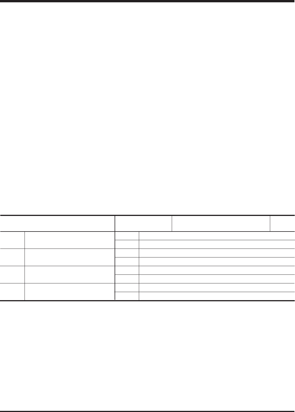
Table 2.6.1 shows the voltage comparator control register Q3.
Table 2.6.1 Voltage comparator control register Q3
Voltage comparator control register Q3
(Note 2)
at reset : 00002 at RAM back-up : state retained
R/W
Voltage comparator (CMP1)
control bit
Voltage comparator (CMP0)
control bit
CMP1 comparison result store bit
CMP0 comparison reslut store bit
Q33
Q32
Q31
Q30
0
1
0
1
0
1
0
1
Notes 1: “R” represents read enabled, and “W” represents write enabled.
2: Bits 0 and 1 of register Q3 can be only read.
Voltage comparator (CMP1) invalid
Voltage comparator (CMP1) valid
Voltage comparator (CMP0) invalid
Voltage comparator (CMP0) valid
CMP1- > CMP1+
CMP1- < CMP1+
CMP0- > CMP0+
CMP0- < CMP0+


