


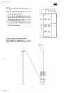
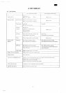
M 7,
3500
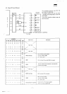
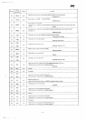
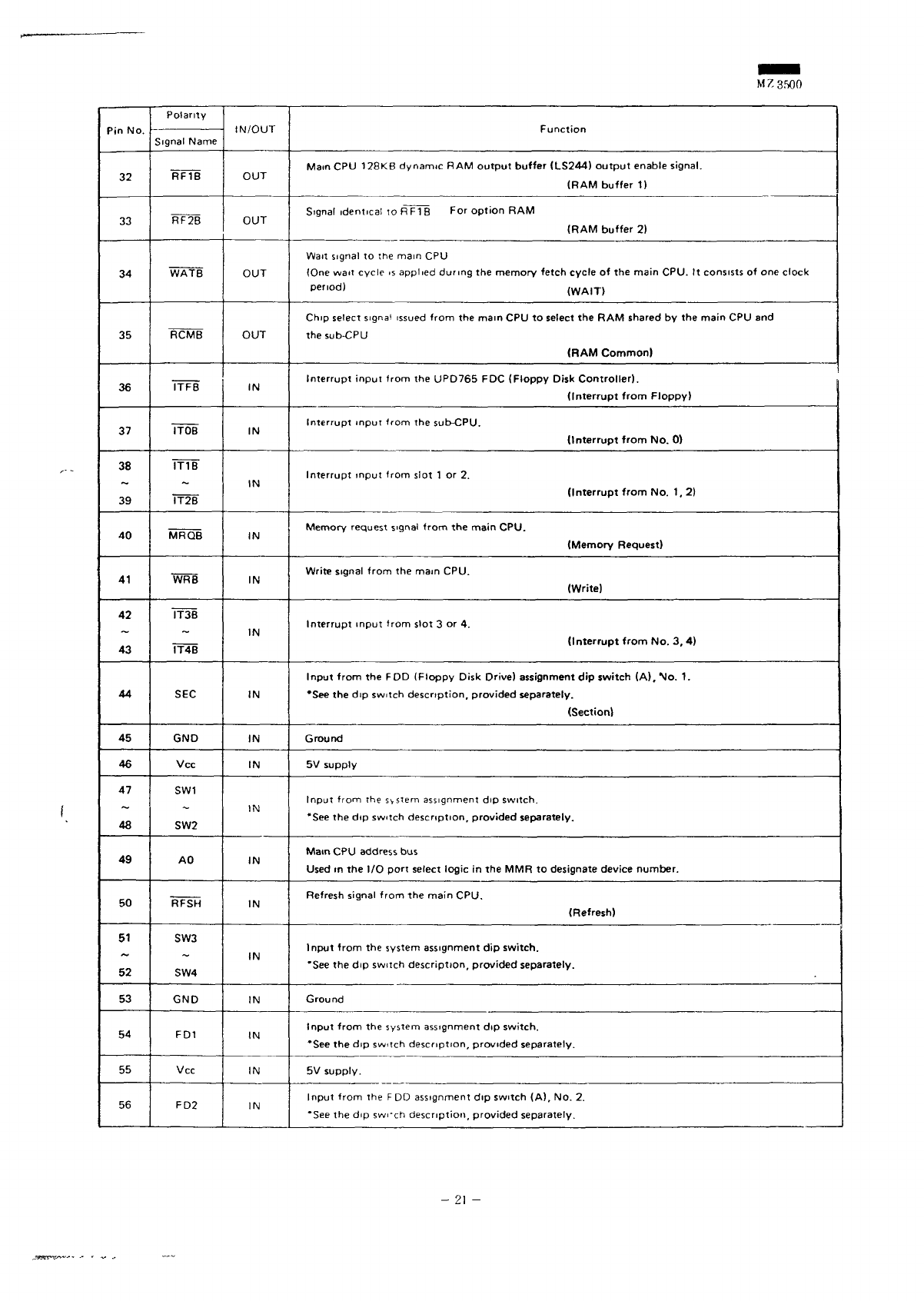
Pin
No.
32
33
34
35
36
37
38
39
40
41
42
43
44
45
46
47
48
49
50
51
52
53
54
55
56
Polarity
Signal
Name
RF1B
RF2B
WATB
RCMB
ITFB
ITOB
IT1B
TT2B
MRQB
WRB
IT3B
IT4B
SEC
GND
Vcc
SW1
SW2
AO
RFSH
SW3
SW4
GND
FD1
Vcc
FD2
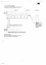
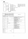
IN/OUT
OUT
OUT
OUT
OUT
IN
IN
IN
IN
IN
IN
IN
IN
IN
IN
IN
IN
IN
IN
IN
IN
IN
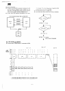
Function
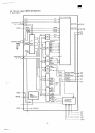
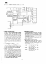
Main
CPU
128KB
dynamic
RAM
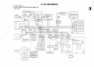
output
buffer
(LS244)
output
enable signal.
(RAM
buffer
1)
Signal
identical
to R F 1 B For
option
RAM
(RAM
buffer
2)
Wait
signal
to the mam CPU
(One
wait
cycle
15
applied during
the
memory fetch cycle
of the
main CPU.
It
consists
of one
clock
period)
(WA|T)
Chip
select
signal
issued
from
the mam CPU to
select
the RAM
shared
by the
main
CPU and
the
sub-CPU
(RAM
Common)
Interrupt
input
from
the
UPD765
FDC
(Floppy
Disk
Controller).
(Interrupt
from
Floppy)
Interrupt
input
from
the
sub-CPU.
(Interrupt
from
No. 0)
Interrupt
input
from slot
1 or 2.
(Interrupt
from
No. 1, 2)
Memory
request signal
from
the
main
CPU.
(Memory
Request)
Write
signal from
the
main CPU.
(Write)
Interrupt
input
from slot
3 or 4.
(Interrupt
from
No. 3, 4)
Input
from
the FDD
(Floppy Disk Drive) assignment
dip
switch
(A),
No. 1.
'See
the dip
switch
description,
provided
separately.
(Section)
Ground
5V
supply
Input from
The
svstem
assignment
dip
switch,
"See
the dip
switch
description,
provided
separately.
Mam CPU
address
bus
Used
rn the I/O
port
select
logic
in the MMR to
designate device
number.
Refresh
signal from
the
main CPU.
(Refresh)
Input
from
the
system
assignment
dip
switch.
•See
the dip
switch
description,
provided
separately.
Ground
Input
from
the
system
assignment
dip
switch.
'See
the dip
switch
description,
provided
separately.
5V
supply.
Input
from
the FDD
assignment
dip
switch (A),
No. 2.
*See
the dip
swi'ch
description, provided
separately.