


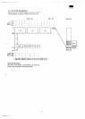
M
7.3500
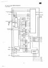
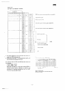
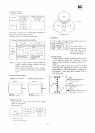
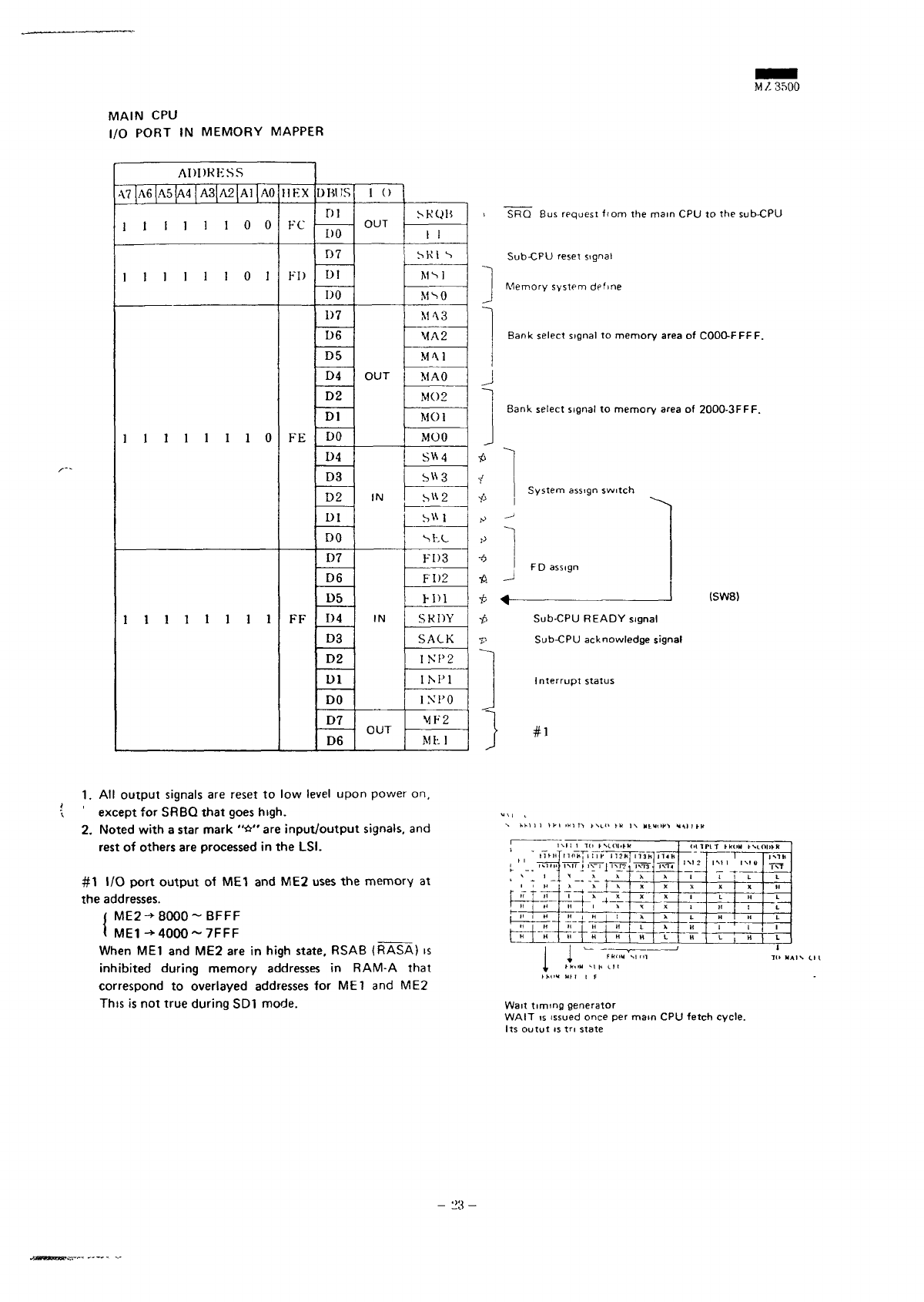
MAIN
CPU
I/O
PORT
IN
MEMORY
MAPPER
ADDKKSS
A7
A6
A5|A4|A3|A2|Al|AO
1
1 1 1 1 1 0 1
11111110
11111111
HEX
KI)
FE
FF
UHUS
01
DO
D7
Dl
DO
1)7
D6
D5
D4
D2
Dl
DO
D4
D3
D2
Dl
DO
D7
D6
D5
1)4
D3
D2
Dl
DO
D7
D6
1
O
r\i IT
OUT
INI
IN
SKQB
1 1
SKI
S
MS]
MSO
M<\3
MA2
MAI
MAO
MO2
MOI
MOO
SW4
b«3
M\2
Sttl
she
FD3
FD2
H>1
SKDY
SACK
1NP2
I
MM
IN'1'0
MF2
Mhl
_J
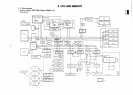
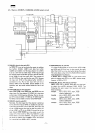
SRQ
Bus
request from
the mam CPU to the
sob-CPU
Sub-CPU
reset signal
Memory
system
define
Bank
select
signal
to
memory
area
of
COOO-FFFF.
Bank
select signal
to
memory
area
of
2000-3FFF.
System
assign
switch
FD
assign
(SW8)
•f>
Sub-CPU READY
signal
•p
Sub-CPU acknowledge
signal
Interrupt
status
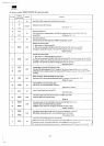
1. All
output
signals
are
reset
to low
level
upon
power
on,
except
for
SRBQ
that
goes
high.
2.
Noted
with
a
star
mark
"£" are
input/output
signals,
and
rest
of
others
are
processed
in the
LSI.
#1 I/O
port
output
of ME1 and ME2
uses
the
memory
at
the
addresses.
(
ME2->8000~BFFF
I
ME1->-4000~7FFF
When
ME1 and ME2 are in
high state.
RSAB
(RASA)
is
inhibited
during memory
addresses
in
RAM-A
that
correspond
to
overlayed
addresses
for MET and ME2
This
is not
true during
SD1
mode.
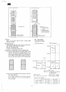
Mm
i i -^.
t
<|
,
"fJ~
11
1 H
" I "
H
j H
M II TO t
MOI«m
n (i H j 1 I 1 H M 2 h
TvfT
J
i\=TjTNT7
1
j X X
H 1 H | 1
H j H j H
Tisn
JM3
H
j H j H | H
1
T4h
01
iri T
hkoM
fMont
IM 2
1
1
1
L
H
H
IM 1
X
L
H
H
|M It
"-
T"
H
I
H
I ' 1
1
h
L
1 H |
i
l
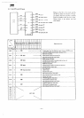
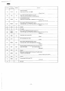
FKOM
SI
in
TO
HA
""•»
M
"
l
"
Wait
timing
generator
WAIT
is
issued once
per
main
CPU
fetch
cycle.
Its
outut
is tri
state