


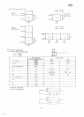

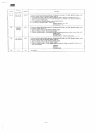
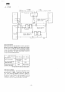
M
7.3500
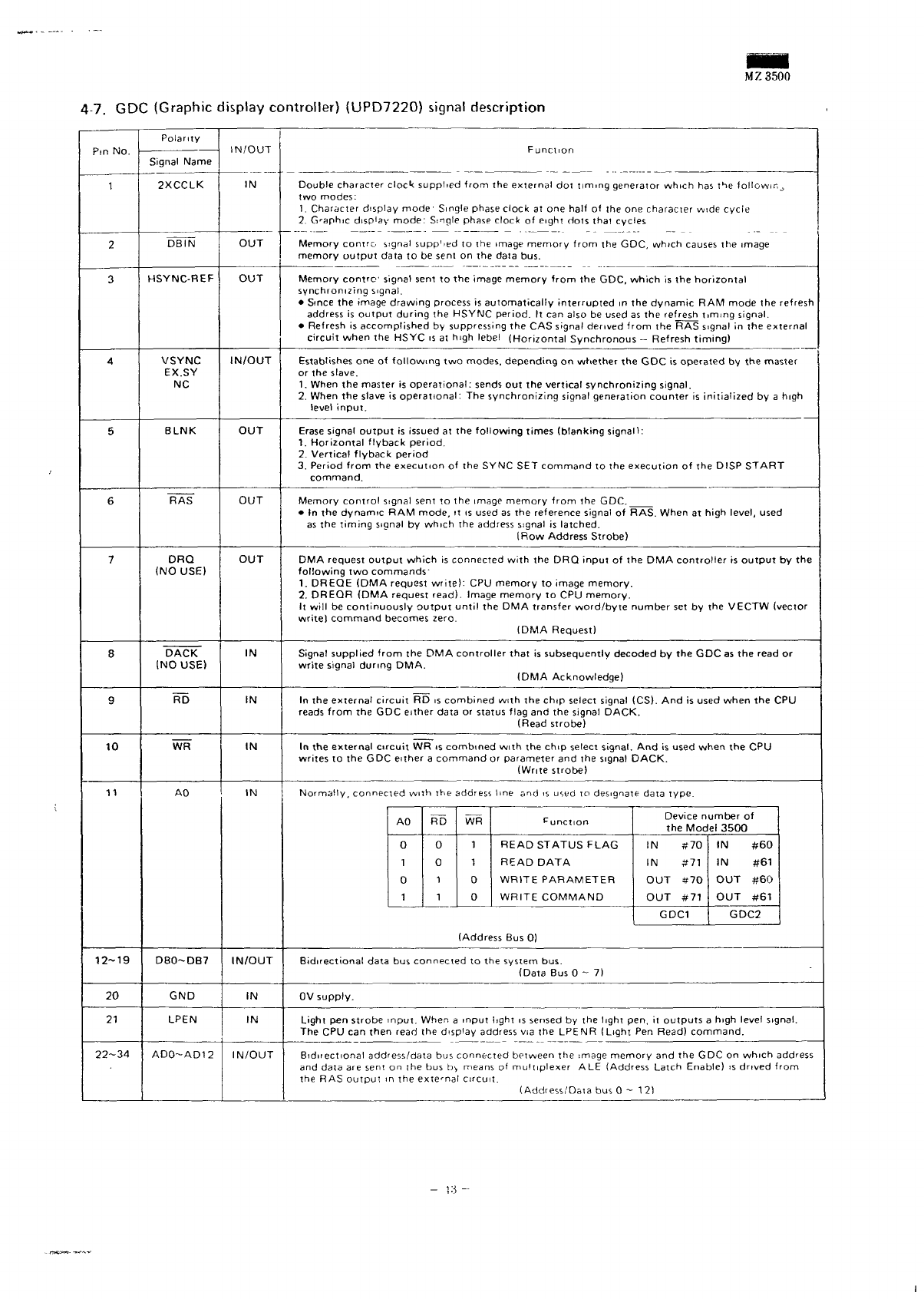
4-7.
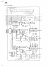
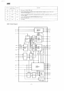
GDC
(Graphic
display
controller)
(UPD7220)
signal
description
1
2
3
4
5
6
7
8
9
10
11
12~19
20
21
22-34
Polarity
Signal
Name
2XCCLK
DBIN
HSYNC-REF
VSYNC
EX.SY
NC
BLNK
RAS
DRQ
(NO
USE)
DACK
(NO
USE)
RD
WR~
AO
DBO-DB7
GND
LPEN
ADO-AD12
IN
OUT
OUT
IN/OUT
OUT
OUT
OUT
IN
IN
IN
IN
IN/OUT
IN
IN
IN/OUT
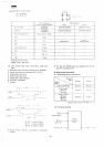
Double
character
clock supplied from
the
external
dot
timing
generator
which
has the
followin^
two
modes:
1.
Character
display
mode
1
Single
phaseclock
at one
half
of the one
character
wide
cycle
2.
G
r
aphic
disp'ay
mode:
Single
phase
clock
of
eight
dots
that
cycles
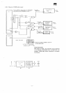
Memory contro
signal
supp'ied
to the
image
memory from
the
GDC, which
causes
the
image
memory
output
data
to be
sent
on the
data
bus.
Memory
contro'
signal sent
to the
image memory
from
the
GDC,
which
is the
horizontal
synchronizing
signal.
•
Since
the
image drawing
process
is
automatically interrupted
in the
dynamic
RAM
mode
the
refresh
address
is
output during
the
HSYNC period.
It can
also
be
used
as the
refresh
timing signal.
•
Refresh
is
accomplished
by
suppressing
the CAS
signal
derived from
the RAS
signal
in the
external
circuit when
the
HSYC
is at h gh
lebel
(Horizontal Synchronous
-
Refresh
timing)
Establishes
one of
following
two
modes,
depending
on
whether
the GDC is
operated
by the
master
or the
slave.
1.
When
the
master
is
operational:
sends
out the
vertical synchronizing signal.
2.
When
the
slave
is
operational
: The
synchronizing
signal
generation counter
is
initialized
by a
high
level
input.
Erase
signal
output
is
issued
at the
following
times (blanking
signal):
1.
Horizontal flyback period.
2.
Vertical flyback period
3.
Period from
the
execution
of the
SYNC
SET
command
to the
execution
of the
DISP START
command.
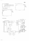
Memory
control
signal
sent
to the
image
memory from
the
GDC,
• In the
dynamic
RAM
mode,
it is
used
as the
reference
signal
of
RAS. When
at
high level, used
as
the
timing
signal
by
which
the
address
signal
is
latched.
(Row Address Strobe)
DMA
request
output
which
is
connected
with
the DRQ
input
of the DMA
controller
is
output
by the
following
two
commands'
1.
DREQE (DMA request write):
CPU
memory
to
image
memory.
2.
DREQR (DMA
request
read).
Image memory
to CPU
memory.
It
will
be
continuously
output
until
the DMA
transfer
word/byte number
set by the
VECTW
(vector
write)
command
becomes zero.
(DMA
Request)
Signal
supplied
from
the DMA
controller that
is
subsequently decoded
by the GDC as the
read
or
write signal
during
DMA.
(DMA Acknowledge)
In the
external circuit
RD is
combined with
the
chip
select
signal
(CS).
And is
used when
the CPU
reads
from
the GDC
either
data
or
status
flag
and the
signal
DACK.
(Read
strobe)
In the
external
circuit
WR is
combined
with
the
chip
select
signal.
And is
used when
the CPU
writes
to the GDC
either
a
command
or
parameter
and the
signal DACK.
(Write
strobe)
Normally, connected
with
the
address
line
and is
used
TO
designate
data
type.
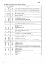
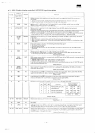
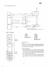
AO
RD WR
function
^Mode^'
0 0 1
READ STATUS FLAG
IN #70 IN #60
1
0 1
READ DATA
IN #71 IN #61
0 1 0
WRITE PARAMETER
OUT #70 OUT #60
1
1 0
WRITE COMMAND
OUT #71 OUT #61
GDC1 GDC2
(Address
Bus 0)
Bidirectional
data
bus
connected
to the
system
bus.
(Data
Bus
0-7)
0V
supply.
Light
pen
strobe
nput.
When
a
input
light
is
sensed
by the
light pen,
it
outputs
a
high
level
signal.
The CPU can
then
read
the
display
address
via the
LPENR
(Light
Pen
Read)
command.
Bidn
ectional
address/data
bus
connected
between
the
image memory
and the GDC on
which
address
and
data
are
sent
on the bus by
means
of
multiplexer
ALE
(Address
Latch
Enable)
is
drived from
the
RAS
output
in the
exte
r
nal
circu
t.
(Address/Data
bus
0-12)