M
7.3 500
5-7.
Precompensate
Circuit
KKITE
DATA
(Fig.
2)
PSO
0
0
1
1
PS1
0
1
0
1
FM
Not
changed
-
-
-
MFM
Not
changed
LATE(125»is)
EARLY(125ja)
-
Value
of LSI 63
1101
1100
1110
-
(Table!)
WDATA-
8MHz
CLOCK
EARLY-
NOMAL-
LATE-
(Fig.3)
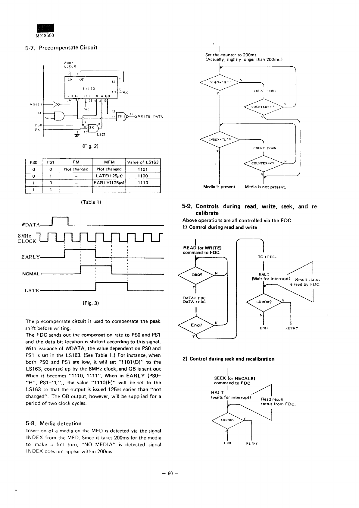
The
precompensate circuit
is
used
to
compensate
the
peak
shift
before
writing.
The FDC
sends
out the
compensation rate
to PSO and PS1
and the
data
bit
location
is
shifted according
to
this
signal.
With
issuance
of
WDATA.
the
value
dependent
on PSO and
PS1
is set in the
LS163. (See Table
1.) For
instance,
when
both
PSO and PS1 are
low,
it
will
set
"1101 (D)"
to the
LS163,
counted
up by the
8MHz
clock,
and QB is
sent
out
When
it
becomes
"1110,
1111".
When
in
EARLY
(PSO=
"H",
PS1="L"),
the
value
"1110(E)"
will
be set to the
LS163
so
that
the
output
is
issued 125ns earier
than
"not
changed".
The QB
output,
however,
will
be
supplied
for a
period
of two
clock
cycles.
5-8. Media detection
Insertion
of a
media
on the MFD is
detected
via the
signal
INDEX from
the
MFD.
Since
it
takes
200ms
for the
media
to
make
a
full turn,
"NO
MEDIA"
is
detected signal
INDEX
does
not
appear
within 200ms.
Set
the
counter
to
200ms.
(Actually, slightly longer than 200ms.)
Media
is
present.
Media
is not
present.
5-9.
Controls
during
read,
write,
seek,
and re-
calibrate
Above operations
are all
controlled
via the
FDC.
1)
Control
during
read
and
write
I
READ
(or
WRITE)
command
to
FDC.
f
I
DATA<-
FDC
DATA-*
FDC
TC-»FDC.
HALT
(Wait
for
interrupt) H-">uit
staius
is
read
by
FDC.
2)
Control during
seek
and
recalibration
SEEK
(or
RECALB)
command
to FDC
I
HALT
(waits
for
interrupt)
Read'result
status
from FDC.
tNI)
RtTKY
-
60
-


