


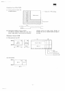
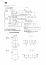
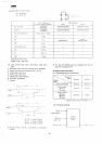
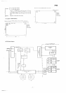

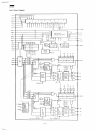

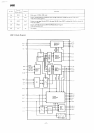
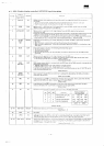
MZ3500
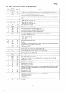
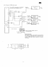
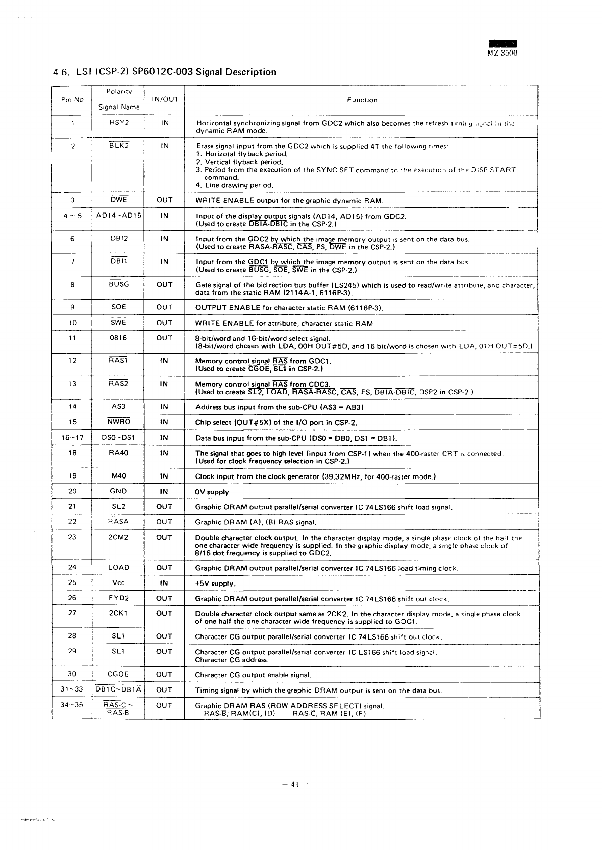
46. LSI
(CSP-2)
SP6012C-003
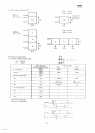
Signal
Description
1
2
3
4-5
6
7
8
9
10
11
12
13
14
15
16-17
18
19
20
21
22
23
24
25
26
27
28
29
30
31-33
34-35
Polarity
Signal
Name
HSY2
BLK2
OWE
AD14-AD15
DBI2
DBI1
BUSG
SOE
SWE
0816
RAS1
RAS2
ASS
NWRO
DSO-DS1
RA40
M40
GND
SL2
RASA
2CM2
LOAD
Vcc
FYD2
2CK1
SL1
SL1
CGOE
DB1C-DB1A
RAS-C
~
RAS-B
IN/OUT
IN
IN
OUT
IN
IN
IN
OUT
OUT
OUT
OUT
IN
IN
IN
IN
IN
IN
IN
IN
OUT
OUT
OUT
OUT
IN
OUT
OUT
OUT
OUT
OUT
OUT
OUT
Horizontal
synchronizing
signal
from
GDC2 which
also
becomes
the
refresh
tirniny
.ijr.s'i
in the
dynamic
RAM
mode.
Erase
signal
input
from
the
GDC2 which
is
supplied
4T the
following
times:
1.
Horizotal flyback period.
2.
Vertical flyback
period.
3.
Period from
the
execution
of the
SYNC
SET
command
to -be
execution
of the
DISP
START
command.
4.
Line drawing period.
WRITE
ENABLE
output
for the
graphic dynamic RAM.
Input
of the
display
output
signals
(AD14,
AD1 5)
from GDC2.
(Used
to
create
DBIA-DBIC
in the
CSP-2.)
Input
from
the
GDC2
by
which
the
image
memory
output
is
sent
on the
data bus.
(Used
to
create
RASA-RASC, CAS,
PS, OWE in the
CSP-2.)
Input
from
the
GDC1
by
which
the
image memory
output
is
sent
on the
data
bus.
(Used
to
create
BUSG, SOE,
SWE in the
CSP-2.)
Gate
signal
of the
bidirection
bus
buffer
(LS245)
which
is
used
to
read/write
attribute,
and
character,
data
from
the
static
RAM (21
14A-1
, 61
16P-3).
OUTPUT
ENABLE
for
character
static
RAM (61
16P-3).
WRITE
ENABLE
for
attribute,
character
static
RAM.
8-bit/word
and
16-bit/word
select
signal.
(8-bit/word
chosen
with
LDA.
OOH
OUT#5D,
and
16-bit/word
is
chosen
with LDA,
01 H
OUTiSD.)
Memory
control
signal
RAS
from
GDC1.
(Used
to
create CGOE,
SL1 in
CSP-2.)
Memory
control
signal
RAS
from
CDC3.
(Used
to
create SL2,
LOAD,
RASA-RASC, CAS,
FS.
DBIA-DBIC.
DSP2
in
CSP-2.)
Address
bus
input
from
the
sub-CPU (ASS
=
AB3)
Chip
select (OUT#5X)
of the I/O
port
in
CSP-2.
Data
bus
input
from
the
sub-CPU (DSO
=
DBO,
DS1 = DB1 ).
The
signal
that
goes
to
high
level
(input
from
CSP-1)
when
the
400-raster
CRT is
connected.
(Used
for
clock
frequency selection
in
CSP-2.)
Clock
input
from
the
clock
generator
(39.32MHz,
for
400-raster mode.)
0V
supply
Graphic DRAM
output
parallel/serial converter
1C
74LS166 shift load
signal.
Graphic
DRAM (A),
(B) RAS
signal.
Double
character
clock
output.
In the
character
display
mode,
a
single
phase
clock
of the
half
the
one
character
wide
frequency
is
supplied.
In the
graphic display mode,
a
single
phase
clock
of
8/16
dot
frequency
is
supplied
to
GDC2.
Graphic
DRAM
output
parallel/serial converter
1C
74LS166
load
timing
clock.
+5V
supply.
Graphic
DRAM
output
parallel/serial
converter
1C
74LS166 shift
out
clock.
Double
character clock
output
same
as
2CK2.
In the
character
display mode,
a
single
phase
clock
of one
half
the one
character wide frequency
is
supplied
to
GDC1
.
Character
CG
output
parallel/serial converter
1C
74LS166 shift
out
clock.
Character
CG
output
parallel/serial
converter
1C
LS166
shift
load
signal.
Character
CG
address.
Character
CG
output
enable signal.
Timing
signal
by
which
the
graphic DRAM output
is
sent
on the
data
bus.
Graphic
DRAM
RAS
(ROW ADDRESS
SELECT)
signal
RAS-B;
RAM(C),
(D)
RAS-C;
RAM
(E),
(F)
-
41
-