MZ3500
9,
POWER
CIRCUIT
DESCRIPTION
1.
BLOCK
DIAGRAM
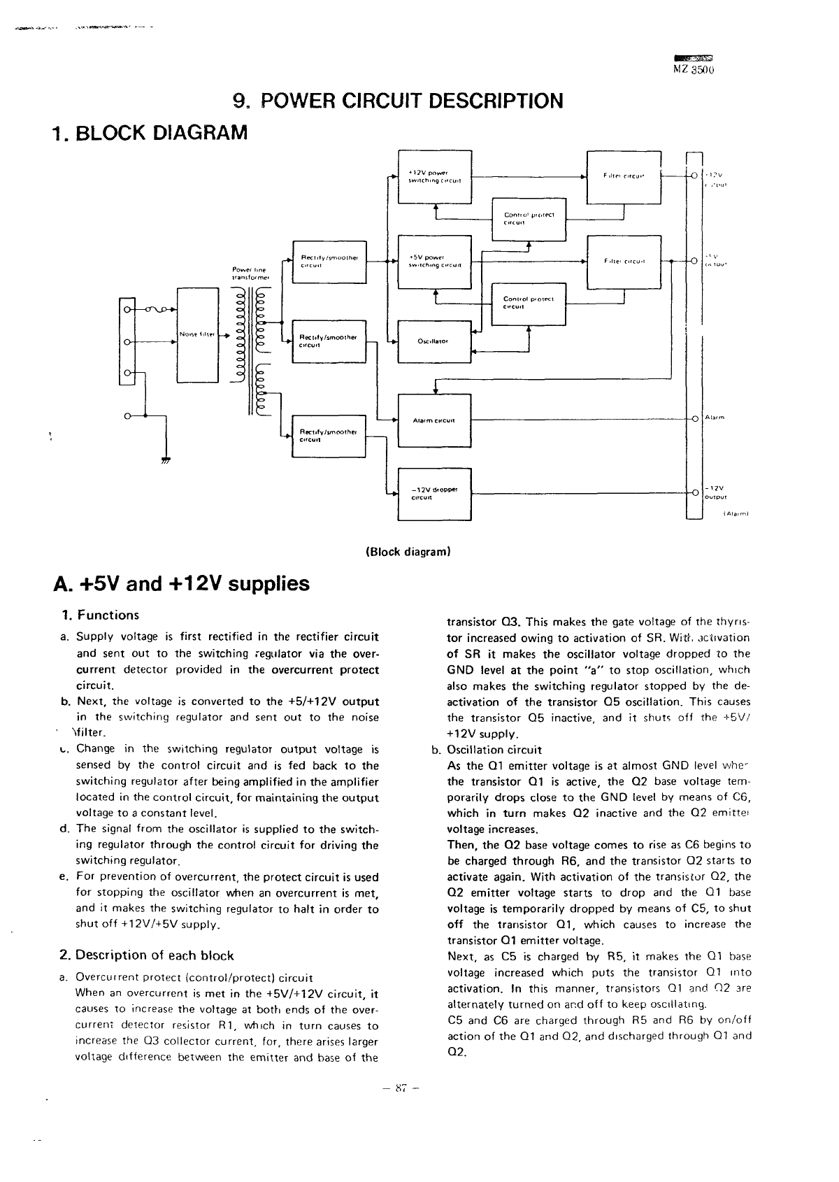
(Block
diagram)
A.
+5V and
+12V
supplies
1.
Functions
a.
Supply
voltage
is
first
rectified
in the
rectifier
circuit
and
sent
out to the
switching
regulator
via the
over-
current
detector
provided
in the
overcurrent
protect
circuit.
b.
Next,
the
voltage
is
converted
to the
+5/+12V
output
in the
switching regulator
and
sent
out to the
noise
•
Nfilter.
c.
Change
in the
switching
regulator
output
voltage
is
sensed
by the
control
circuit
and is fed
back
to the
switching regulator after being
amplified
in the
amplifier
located
in the
control
circuit,
for
maintaining
the
output
voltage
to a
constant level.
d. The
signal
from
the
oscillator
is
supplied
to the
switch-
ing
regulator
through
the
control
circuit
for
driving
the
switching regulator.
e.
For
prevention
of
overcurrent,
the
protect
circuit
is
used
for
stopping
the
oscillator when
an
overcurrent
is
met,
and
it
makes
the
switching regulator
to
halt
in
order
to
shut
off
+12V/+5V
supply.
2.
Description
of
each
block
a.
Overcutrent protect (control/protect)
circuit
When
an
overcurrent
is met in the
+5V/+12V
circuit,
it
causes
to
increase
the
voltage
at
both
ends
of the
over-
current
detector
resistor
R1,
which
in
turn
causes
to
increase
the Q3
collector current, for, there
arises
larger
voltage difference between
the
emitter
and
base
of the
transistor
Q3.
This
makes
the
gate voltage
of the
thyns-
tor
increased
owing
to
activation
of SR.
Witr,
jctivation
of SR it
makes
the
oscillator
voltage dropped
to the
GND
level
at the
point
"a" to
stop oscillation,
which
also
makes
the
switching
regulator stopped
by the de-
activation
of the
transistor
Q5
oscillation.
This
causes
the
transistor
Q5
inactive,
and it
shuts
off the
+5V/
+ 12V
supply,
b.
Oscillation
circuit
As
the Q1
emitter
voltage
is at
almost
GND
level
whe-
the
transistor
Q1 is
active,
the Q2
base
voltage tem-
porarily
drops
close
to the GND
level
by
means
of C6,
which
in
turn
makes
Q2
inactive
and the Q2
emittei
voltage increases.
Then,
the Q2
base
voltage comes
to
rise
as C6
begins
to
be
charged
through
R6, and the
transistor
Q2
starts
to
activate again.
With
activation
of the
transistor
Q2, the
Q2
emitter
voltage starts
to
drop
and the Q1
base
voltage
is
temporarily
dropped
by
means
of C5, to
shut
off the
transistor
Ql,
which
causes
to
increase
the
transistor
Q1
emitter
voltage.
Next,
as C5 is
charged
by R5, it
makes
the Q1
base
voltage
increased
which
puts
the
transistor
Ql
into
activation.
In
this manner,
transistors
Q1 and O2 are
alternately
turned
on and off to
keep oscillating.
C5 and C6 are
charged
through
R5 and R6 by
on/off
action
of the Q1 and Q2, and
discharged
through
Ql and
Q2.


