


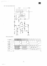
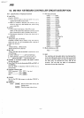
M23500
c.
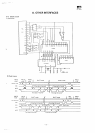
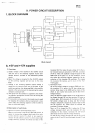
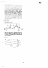
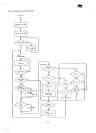
Power
switching
circuit
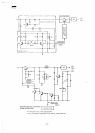
As
the
signal
from
the
oscillator
is
amplified
through
Q7
to Q6 to
change
current
to the
transformer
T2. it
causes
voltage
to
appear
on the
base
of Q5
(one
of
components
is
cut by
D1),
so
that
the
transistor
Q5
begins
to
per-
form switching operation
in
synchronization
with
the
oscillation
frequency.
As Q2 is
switched,
current
is
supplied
to the
emitter
side
of the
transistor
Q5,
which
produces
smoothed
voltage
through
the
capacitor
C1
and the
coil
L2. The
circuit
composed
of D4 and VR1 is
the
reference
voltage
for the +5 or + 12V
supply,
which
is
used
to
control
the
emitter
current
flowing
to the
transistor
Q9. The
current
supplied
from
Q9 is
used
to
create
Tr3
inactive
by the
delayed
C1 and C2
voltages
which
supplied from Tr1-R2-VR1-D3.
It
goes
high
with
deactivation
of
Tr3.
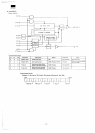
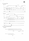
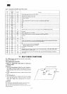
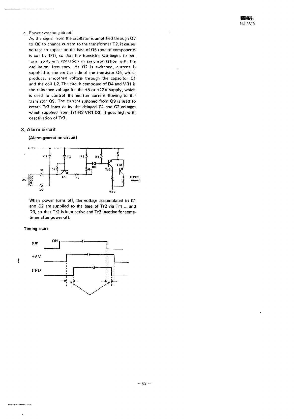
3.
Alarm circuit
(Alarm generation
circuit)
When power
turns
off,
the
voltage
accumulated
in C1
and
C2 are
supplied
to the
base
of Tr2 via Tr1 ... and
D3, so
that
Tr2 is
kept
active
and Tr3
inactive
for
some-
times
after
power
off.
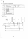
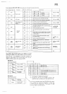
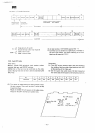
Timing chart
SW
+ 5V
PFD
-89
-