


MZ
3500
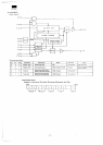
6-6. 8253
Controls
Baud
rate
of
this
interface
will
be
determined
by the
clock
output
of the
8253.
The
8251
is
configured such
that
its
baud
rate
is
1/16
of the
input
clock
and has the
following
relation
between
the
8253
output
clock
and the
baud
rate:
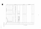
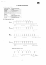
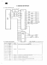
8253
input
frequency:
2457.6kHz
8253
Mode set: Mode 3(rec'angle waveform
rate
generator)
Control
signals
Baud
rale
1
1 0 .t -
300
600
1
200
2400
4800
9600
8253
Output
frequency
1760
H
z
4800
9600
1
9200
38400
76800
153600
8253
Parameter
1
3 9 6.3 6
51 2
256
128
64
32
1
6
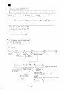
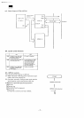
Signal
name
Transmission
enabled
Data
set
ready
Carrier
detect
Ready
Equipment
ready
Paper
out
Symbol
CS
DR
CD
READY
ER
PO
IN/OUT
-*
Peripheral
—
Peripheral
—
Peripheral
—
Peripheral
«-
Peripheral
<-
Peripheral
Function
When
high,
data
input from
a
peripheral
is
enabled.
When
low,
data
input from
a
peripheral
is
disabled.
Goes
high when power
is on to the
interface
unit.
(SW6-ON)
High
at all
times
when power
is on to the
interface
unit.
(SW6-OFF)
Goes
high only when data
is on
output.
Data
output from
the
interface
is
enabled.
(ON)
Data
is
output
from
the
interface.
(OFF)
Waits
for
data
output.
NOTE:
A
maximum
of two
bytes
are
output
after
the
signal
goes
from high
to low
state.
Indicates
that
the
peripheral
is
ready.
It
results
in an
error
if low or
open when data
is
sent
from
the
interface.
This
signal
will
be
invalidated when
the SW5 is
turned
off.
(SW7-ON)
Causes
an
error
if set
high during data
output.
(SW7-OFF)
Causes
an
error
if set low
during
data
output.
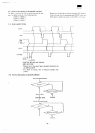
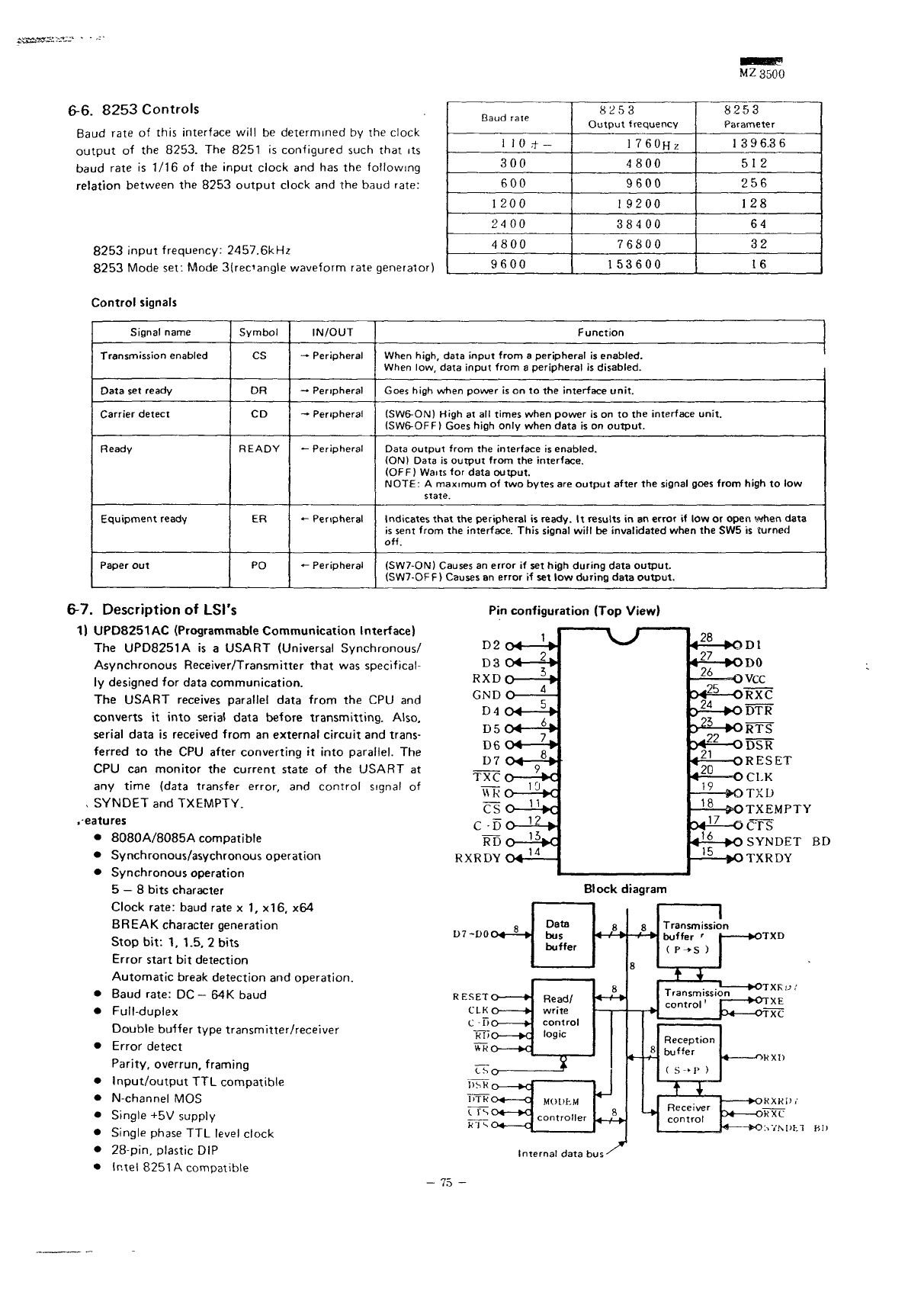
6-7.
Description
of
LSI's
1)
UPD8251AC
(Programmable
Communication
Interface)
The
UPD8251A
is a
USART (Universal Synchronous/
Asynchronous Receiver/Transmitter
that
was
specifical-
ly
designed
for
data
communication.
The
USART
receives
parallel data
from
the CPU and
converts
it
into
serial data
before
transmitting.
Also,
serial
data
is
received
from
an
external
circuit
and
trans-
ferred
to the CPU
after converting
it
into
parallel.
The
CPU
can
monitor
the
current
state
of the
USART
at
any
time
(data
transfer
error,
and
control
signal
of
,
SYNDETandTXEMPTY.
,-eatures
•
8080A/8085A
compatible
•
Synchronous/asychronous
operation
•
Synchronous operation
5
—
8
bits
character
Clock rate: baud
rate
x 1,
x16,
x64
BREAK
character
generation
Stop
bit:
1,
1.5,
2
bits
Error start
bit
detection
Automatic
break
detection
and
operation.
•
Baud rate:
DC
-
64K
baud
•
Full-duplex
Double
buffer
type transmitter/receiver
•
Error detect
Parity, overrun, framing
•
Input/output
TTL
compatible
•
N-channel
MOS
•
Single
+5V
supply
•
Single
phase
TTL
level
clock
•
28-pin,
plastic
DIP
•
Intel
8251A compatible
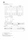
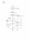
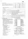
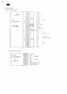
Pin
configuration (Top
View)
<
28
»OD1
3?
5
PORTS'
422-0
DSR
-i-2—XDTXEMPTY
3*12-0
CT3
SYNDET
BD
TXRDY
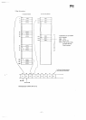
Block diagram
1)7-1)004
8
»
RESET
O »•
Data
bus
buffer
Read/
write
control
logic
*
Dsko
m
t
rscx
—
x:
k'l so* c
MOOhM
controller
8
8
^_
8
V
Internal
data
bus^
„«.
8
8
^
1
Transmission
t *
Transmissic
control
'
Reception
buffer
(
S -• P )
t
1
Receiver
control
>n
_
X>TXE
34
OTXC
HI)
-
75
-