


P R E L I M I N A R Y
AMD
109Am79C930
In addition, the USER5/IRQ4 pin may be used to produce interrupts
to the 80188 embedded controller. This capability is controlled by
the ENXCHBSY bit of TCR28 and the CHBSYCU bit of TIR5 and
operates independently of the bits mentioned above.
The control of the function of the USER5/IRQ4 pin is described in
the
Multi-Function Pin
section.
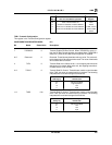
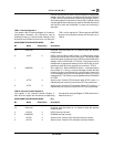
4–3 U1INTCNT 00b USER1 Interrupt control bits. The USER1/IRQ12 pin can be used
to signal an interrupt to the 80188 embedded controller. The
U1INTCNT bits have the following interpretation and operate inde-
pendently of the operating mode of the Am79C930 device (i.e.,
the U1INTCNT bits operate in both PCMCIA and ISA Plug and
Play modes.):
U1INT Bit
U1INTCNT USER1 Pin (TCR11[3])
TCR7[4:3] Event Result
00 X 0 => interrupt
disabled
01 rising edge 1 => interrupt
signaled
10 falling edge 1 => interrupt
signaled
11 rising or 1 => interrupt
falling edge signaled
Note that the USER1 pin function has no effect on the use of the
USER1/IRQ12 pin as an interrupt signaling pin. If the
USER1/IRQ12 pin is to be used as a 80188 controller interrupt
source in the ISA Plug and Play mode, then it is imperative that the
ISA Plug and Play resource data structure loaded into the accom-
panying flash device as part of the Am79C930 device based design
should not include IRQ12 as a choice of IRQ level for possible se-
lection by the ISA Plug and Play configuration software. When this
procedure is followed, then the system designer can be assured
that the IRQ12 function will not be used by the Am79C930 device,
and therefore, the USER1/IRQ12 pin will remain in the high-imped-
ance state and will be available for connection to an interrupt gener-
ating source in the design.
2 TXCMDT 0 TXCMD Data. The value written to the TXCMDT bit is used in some
modes to determine the output value of the TXCMD/LA21 pin.
Reads from TXCMDT always return the current value of the
TXCMD/LA21 pin.
The control of the function of the TXCMD/LA21 pin is described in
the
Multi-Function Pin
section.
1 ANTSLTLD 1 ANTSLTL Data. The value that is written to this bit will be driven out
to the ANTSLT pin of the Am79C930 device when the ANTSLTLFN
bit of TCR30 has been set to a 1 and the ANTSLTLEN bit of TCR15
has also been set to a 1 and the PCMCIA pin is set to 1. The value
that is read from this bit represents the current value of the ANTSLT
pin of the Am79C930 device.
A complete description of the control of the function of the ANTSLT
pin is described in the
Multi-Function Pin
section.
0 TXDATALD 1 TXDATAL Data. The value that is written to this bit will be driven out
to the TXDATA pin of the Am79C930 device when the TXDATALFN
bit of TCR30 has been set to a 1 and the TXDATALEN bit of TCR15