AMD
P R E L I M I N A R Y
76
Am79C930
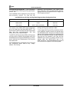
The MIR space contains 16 registers which are used by
the firmware to control allow communication between
the firmware (MAC layer) and the device driver. This
register set also contains the power down registers.
These registers are only accessible through the 80188
core; they are inaccessible from the system interface.
The TIR space contains 32 registers which are used by
the 80188 core to control the Am79C930 device’s TAI
unit, to collect TAI status, and to transfer data to and
from the TAI. These registers are accessible from both
the system interface and the 80188 core.
The TCR space contains 32 registers which are used by
the 80188 core to define the functionality of the
Am79C930 device’s TAI unit. These registers are indi-
rectly accessible from both the system interface and the
80188 core through an address and data port that are
part of the TIR set of registers.
The PCMCIA register set consists of two Card Configu-
ration Registers (CCR) and the Configuration Informa-
tion Space (CIS). Full support of the PCMCIA standard
(version 2.1) is facilitated through these registers. The
CCR space is only accessible through the system inter-
face. The CIS space is accessible from both the system
interface and from the 80188 core, although the 80188
core should never need to access the CIS.
The ISA Plug and Play register set consists of three ba-
sic registers which allow an indirect access to an addi-
tional 19 Plug and Play configuration registers plus a
double indirect access to 1K–16 bytes of Plug and Play
Resource Data space. The Plug and Play register space
is only accessible through the system interface, except
that the Resource Data space is also mapped into a por-
tion of the 80188 core memory space.
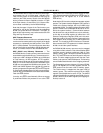
Note that all register locations are defined to be 8 bits
in width.
Some register bits indicate the value “pin” for their de-
fault reset value. Such register bits have a pin as an op-
tional data source and such pins are by default defined
as inputs; hence, the register bit value of “pin” indicates
that the default register bit value depends upon the
value of a pin and is therefore system dependent.
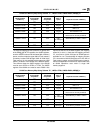
Some register bits indicate the value “–” for their default
reset value. Such register bits have an undefined default
value, even though repeated read accesses may yield a
consistent result for some bit locations thus marked.
AMD reserves the right to modify the behavior of these
bits at any time in the future (such as in a revision of this
device) and, therefore, all values read from these loca-
tions should be regarded as unknown until such time as
a use has been assigned to them. Note also that all such
bits have a write value that must be used when write
accesses to other bit locations in the register occur. This
write value is usually 0. Users must strictly obey
prescribed write values to avoid future software
incompatibility problems.
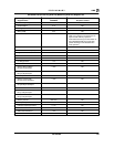
System Interface Registers (SIR space)
The SIR space contains eight registers which are used
by the host driver to control Am79C930 device opera-
tions and to collect status, namely, the General Configu-
ration Register and the Bank Switching Select Register.
The Local Memory Address and Local Memory Data
registers may be used instead of system-memory-
mapped transfers to SRAM locations in order to elimi-
nate the need for system memory space allocation.
These registers are only accessible at the system inter-
face; they are inaccessible from the 80188 core.


